M15T4G8512A-DEBG2S
M15T4G8512A-DEBG2S is 64M x 8 Bit x 8 Banks DDR3 SDRAM manufactured by Elite Semiconductor Microelectronics Technology.
- Part of the M15T4G8512A comparator family.
- Part of the M15T4G8512A comparator family.
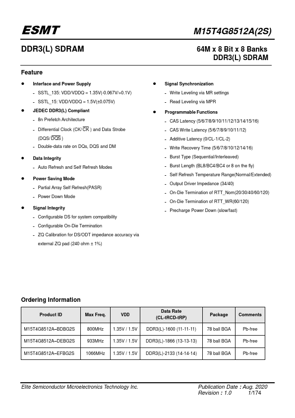
ESMT
DDR3(L) SDRAM
Feature
- Interface and Power Supply ˗ SSTL_135: VDD/VDDQ = 1.35V(-0.067V/+0.1V) ˗ SSTL_15: VDD/VDDQ = 1.5V(±0.075V)
- JEDEC DDR3(L) pliant ˗ 8n Prefetch Architecture ˗ Differential Clock (CK/ CK ) and Data Strobe (DQS/ DQS ) ˗ Double-data rate on DQs, DQS and DM
- Data Integrity ˗ Auto Refresh and Self Refresh Modes
- Power Saving Mode ˗ Partial Array Self Refresh(PASR) ˗ Power Down Mode
- Signal Integrity ˗ Configurable DS for system patibility ˗ Configurable On-Die Termination ˗ ZQ Calibration for DS/ODT impedance accuracy via external ZQ pad (240 ohm ± 1%)
M15T4G8512A(2S)
64M x 8 Bit x 8 Banks DDR3(L) SDRAM
- Signal Synchronization ˗ Write Leveling via MR...