M15T5121632A-DEBG
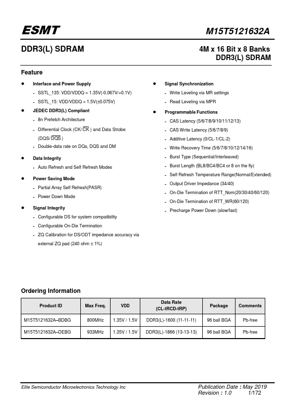
M15T5121632A-DEBG is 4M x 16-Bit x 8 Banks DDR3 SDRAM manufactured by Elite Semiconductor Microelectronics Technology.
- Part of the M15T5121632A comparator family.
- Part of the M15T5121632A comparator family.
Feature
- Interface and Power Supply ˗ SSTL_135: VDD/VDDQ = 1.35V(-0.067V/+0.1V) ˗ SSTL_15: VDD/VDDQ = 1.5V(±0.075V)
- JEDEC DDR3(L) pliant ˗ 8n Prefetch Architecture ˗ Differential Clock (CK/ CK ) and Data Strobe (DQS/ DQS ) ˗ Double-data rate on DQs, DQS and DM
- Data Integrity ˗ Auto Refresh and Self Refresh Modes
- Power Saving Mode ˗ Partial Array Self Refresh(PASR) ˗ Power Down Mode
- Signal Integrity ˗ Configurable DS for system patibility ˗ Configurable On-Die Termination ˗ ZQ Calibration for DS/ODT impedance accuracy via external ZQ pad (240 ohm ± 1%)
M15T5121632A
4M x 16 Bit x 8 Banks DDR3(L) SDRAM
- Signal Synchronization ˗ Write Leveling via MR settings ˗ Read Leveling via MPR
- Programmable Functions ˗ CAS Latency (5/6/7/8/9/10/11/12/13) ˗ CAS Write Latency (5/6/7/8/9) ˗ Additive Latency (0/CL-1/CL-2) ˗ Write Recovery Time (5/6/7/8/10/12/14/16) ˗ Burst Type (Sequential/Interleaved) ˗ Burst Length (BL8/BC4/BC4 or 8 on the fly) ˗ Self Refresh Temperature Range(Normal/Extended) ˗ Output Driver Impedance (34/40) ˗ On-Die Termination of RTT_Nom(20/30/40/60/120) ˗ On-Die Termination of RTT_WR(60/120) ˗ Precharge Power Down (slow/fast)
Ordering Information
Product ID
Max Freq.
Data Rate (CL-t RCD-t RP)
M15T5121632A- BDBG
800MHz 1.35V / 1.5V DDR3(L)-1600 (11-11-11)
M15T5121632A- DEBG
933MHz 1.35V / 1.5V DDR3(L)-1866 (13-13-13)
Package ments
96 ball BGA 96 ball BGA
Pb-free Pb-free
Elite Semiconductor Microelectronics Technology Inc
Publication Date : May 2019
Revision : 1.0
1/172
ESMT
M15T5121632A
Description
The 512Mb Double-Data-Rate-3 (DDR3(L)) DRAM is double data rate architecture to achieve high-speed operation. It is internally configured as an eight-bank DRAM.
The 512Mb chip is organized as 4Mbit x 16 I/Os x 8 bank devices. These synchronous devices achieve high speed double-data-rate transfer rates of up to 1866 Mb/sec/pin for general applications.
The chip is designed to ply with all key DDR3(L) DRAM key features and all of the...


