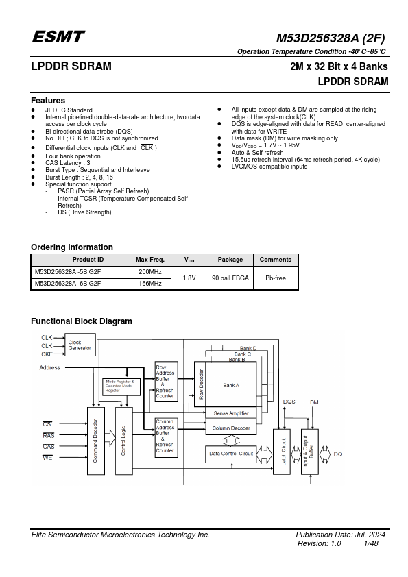
Datasheet4U Logo Datasheet4U.com

M53D256328A-6BIG2F - 2M x 32 Bit x 4 Banks LPDDR SDRAM

Download the M53D256328A-6BIG2F datasheet PDF. This datasheet also covers the M53D256328A variant, as both devices belong to the same 2m x 32 bit x 4 banks lpddr sdram family and are provided as variant models within a single manufacturer datasheet.

General Description

Ball Name Function A0~A11, BA0~BA1 Address inputs - Row address A0~A11 - Column address A0~A8 A10/AP : AUTO Precharge BA0~BA1: Bank selects (4 Banks) DQ0~DQ31 Data-in/Data-out RAS CAS WE VSS VDD DQS0~DQS3 Row address strobe Column address strobe Write enable Ground Power Bi-directional Data S

Key Features

  • JEDEC Standard.
  • Internal pipelined double-data-rate architecture, two data access per clock cycle.
  • Bi-directional data strobe (DQS).
  • No DLL; CLK to DQS is not synchronized.
  • Differential clock inputs (CLK and CLK ).
  • Four bank operation.
  • CAS Latency : 3.
  • Burst Type : Sequential and Interleave.
  • Burst Length : 2, 4, 8, 16.
  • Special function support - PASR (Partial Array Self Refresh) - Internal TCSR (Temperature Compensated Self Refresh) - DS (Drive.

📥 Download Datasheet

Note: The manufacturer provides a single datasheet file (M53D256328A-ESMT.pdf) that lists specifications for multiple related part numbers.

Full PDF Text Transcription (Reference)

The following content is an automatically extracted verbatim text from the original manufacturer datasheet and is provided for reference purposes only.

View original datasheet text
ESMT LPDDR SDRAM Features  JEDEC Standard  Internal pipelined double-data-rate architecture, two data access per clock cycle  Bi-directional data strobe (DQS)  No DLL; CLK to DQS is not synchronized.