145406
feature true TTL input patibility, slew- rate- limited output, 300- Ω power- off source impedance, and output typically switching to within 25% of the supply rails. The receivers can handle up to ± 25 V while presenting 3 to 7 kΩ impedance. Hysteresis in the receivers aids reception of noisy signals. By bining both drivers and receivers in a single CMOS chip, the MC145406 provides efficient, low- power solutions for EIA 232- E and V.28 applications.
Drivers
- ± 5 V to ±12 V Supply Range
- 300- Ω Power- Off Source Impedance
- Output Current Limiting
- TTL patible
- Maximum Slew Rate = 30 V/µs
Receivers
- ± 25 V Input Voltage Range When VDD = 12 V, VSS =
- 12 V
- 3 to 7 kΩ Input Impedance
- Hysteresis on Input Switchpoint
MC145406
16 1
16 1
P SUFFIX PLASTIC CASE 648
DW SUFFIX SOG
CASE 751G
SD SUFFIX SSOP
CASE 940B
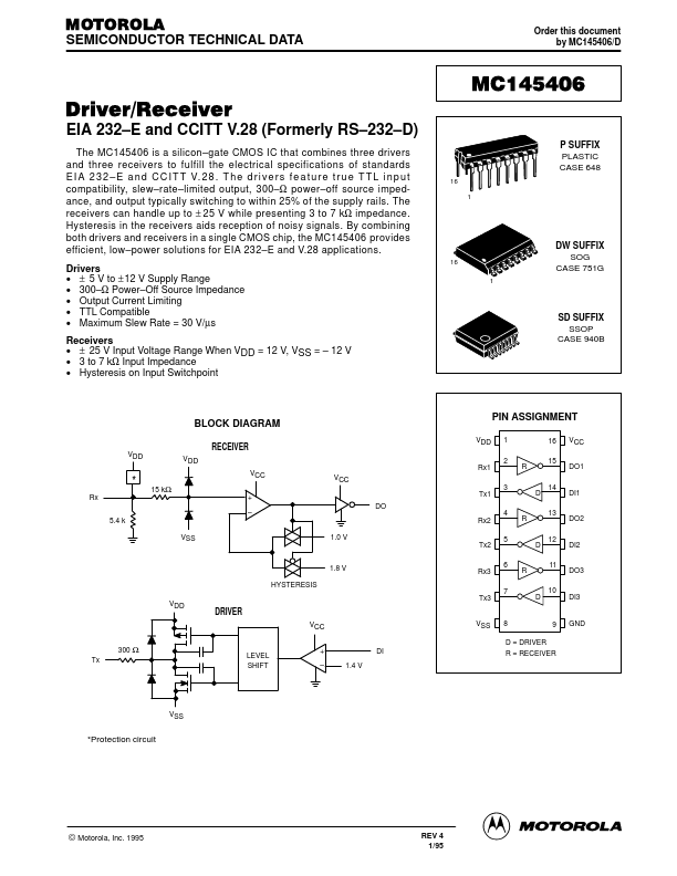
BLOCK DIAGRAM
RECEIVER VDD
- 15 kΩ Rx
VCC +
- 5.4 k
VCC 1.0 V
1.8 V HYSTERESIS
VDD DRIVER
300 Ω Tx
LEVEL SHIFT
+ DI
- 1.4 V
PIN ASSIGNMENT
VDD...