DESCRIPTION
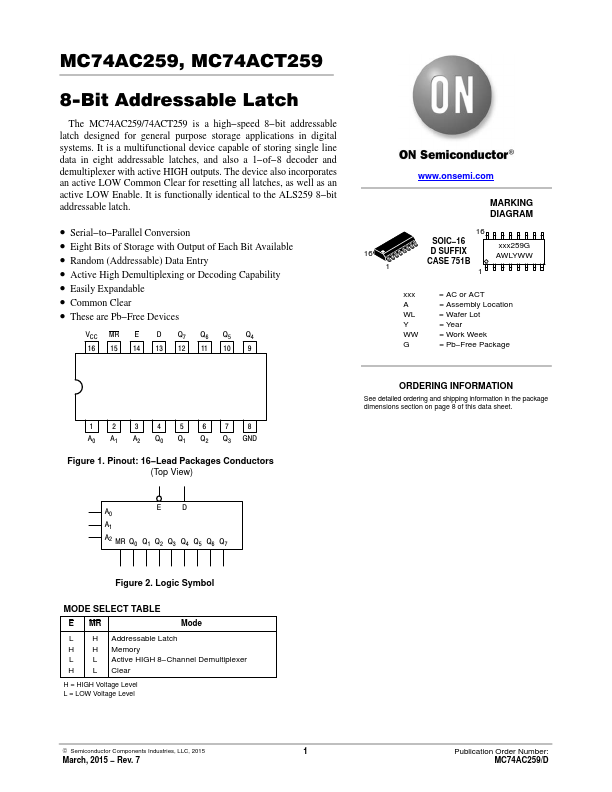
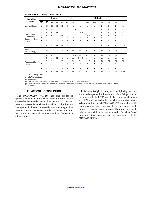
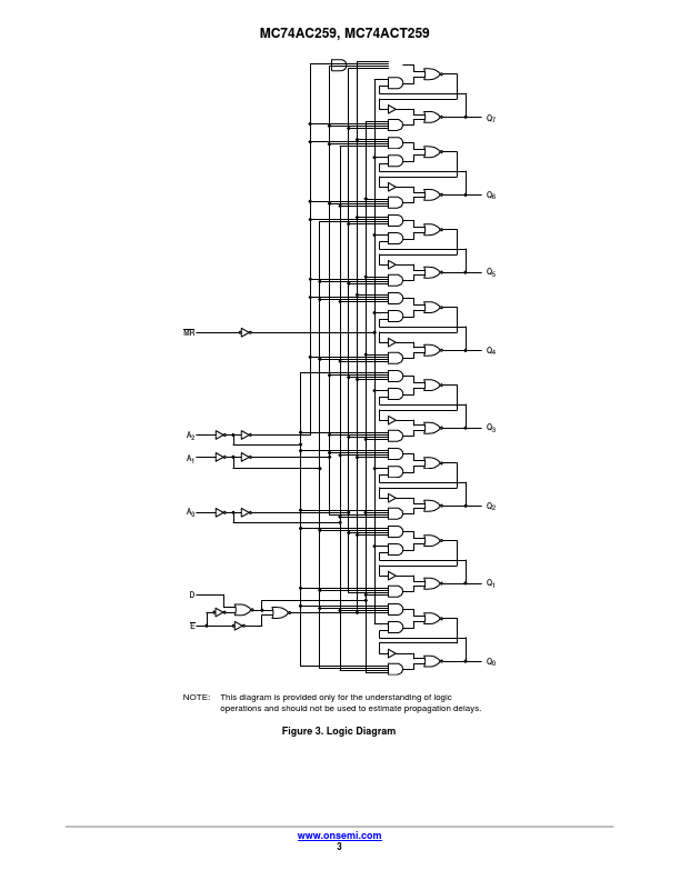
In the addressable latch mode, data on the Data line (D) is written into the addressed latch. All latches remain in their previous state and are unaffected by the Data or Address inputs. In the one−of−eight decoding or demultiplexing mode, the addressed output will follow the state of the D input with all other outputs in the LOW state. In the clear mode all outputs are LOW and unaffected by the address and data inputs. When operating the MC74AC/ACT259 as an addressable latch, changing more than one bit of the address could impose a transient wrong address. Therefore, this should only be done while in the memory mode. The Mode Select Function Table summarizes the operations of the MC74AC/ACT259. 2 MC74AC259, MC74ACT259 Q7 Q6 Q5 MR Q4 A2 Q3 A1 A0 Q2 Q1 D E Q0 NOTE: This diagram is provided only for the understanding of logic operations and should not be used to estimate propagation delays. Figure 3. Logic Diagram 3 MC74AC259, MC74ACT259 MAXIMUM RATINGS
Symbol Parameter Value...