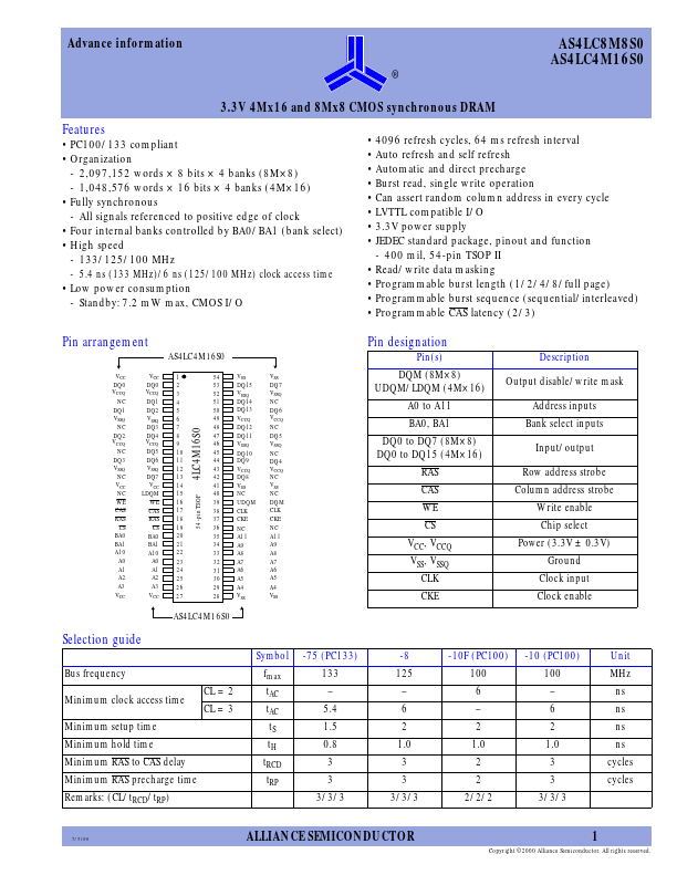
AS4LC8M8S0
AS4LC8M8S0 is 3.3V 4Mx16 and 8Mx8 CMOS synchronous DRAM manufactured by Unknown Manufacturer.
Advance information
®
AS4LC8M8S0 AS4LC4M16S0
3.3V 4Mx16 and 8Mx8 CMOS synchronous DRAM
Features
- PC100/133 pliant
- Organization
- 2,097,152 words × 8 bits × 4 banks (8M×8)
- 1,048,576 words × 16 bits × 4 banks (4M×16)
- Fully synchronous
- All signals referenced to positive edge of clock
- Four internal banks controlled by BA0/BA1 (bank select)
- High speed
- 133/125/100 MHz
- 5.4 ns (133 MHz)/6 ns (125/100 MHz) clock access time
- Low power consumption
- Standby: 7.2 mW max, CMOS I/O
- 4096 refresh cycles, 64 ms refresh interval
- Auto refresh and self refresh
- Automatic and direct precharge
- Burst read, single write operation
- Can assert random column address in every cycle
-...