BISS0001 Overview
Description
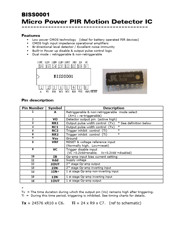
Retriggerable & non-retriggerable mode select (A=1 : re-triggerable) Detector output pin (active high) Output pulse width control (Tx) * See definition below Output pulse width control (Tx) * Trigger inhibit control (Ti) * Trigger inhibit control (Ti) * Ground RESET & voltage reference input (Normally high. Low=reset) Trigger disable input (VC >0.2Vdd=enable; Vc<0.2Vdd =disabled) Op-amp input bias current setting Supply voltage 2nd stage Op-amp output 2nd stage Op-amp inverting input 1 st stage Op-amp non-inverting input 1 st stage Op-amp inverting input 1 st stage Op-amp output * Tx = The time duration during which the output pin (Vo) remains high after triggering.
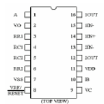
Representative BISS0001 image (package may vary by manufacturer)