IW4093B
TECHNICAL DATA
Quad 2-Input NAND Schmitt Triggers
High-Voltage Silicon-Gate CMOS
The IW4093B consists of four Schmitt-trigger circuits. Each circuit functions as a two-input NAND gate with Schmitt-trigger action on both inputs. The gate switches at different points for positive- and negative- going signals. The difference between the positive voltage (VP) and the negative voltage (VN) is defined as hysteresis voltage (VH) (see Fig.1).
- Operating Voltage Range: 3.0 to 18 V
- Maximum input current of 1 µA at 18 V over full packagetemperature range; 100 n A at 18 V and 25°C
- Noise margin (over full package temperature range): 1.0 V min @ 5.0 V supply 2.0 V min @ 10.0 V supply 2.5 V min @ 15.0 V supply
ORDERING INFORMATION IW4093BN Plastic IW4093BD SOIC TA = -55° to 125° C for all packages
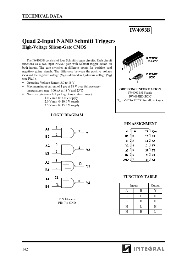
LOGIC DIAGRAM PIN ASSIGNMENT
FUNCTION TABLE
Inputs A L PIN 14 =VCC PIN 7 = GND L H H B L H L H Output Y H H H L
MAXIMUM RATINGS-
Symbol VCC VIN VOUT IIN PD PD Tstg TL
-...