MS8870
MS8870 is DTMF Receiver manufactured by Unknown Manufacturer.
MOSA ELECTRONICS
Features
- -
- -
- plete DTMF receiver Low power consumption Adjustable guard time Central Office Quality CMOS, Single 5V operation O
..
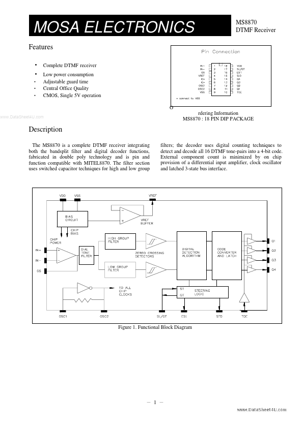
MS8870 DTMF Receiver rdering Information MS8870 : 18 PIN DIP PACKAGE
Description
The MS8870 is a plete DTMF receiver integrating both the bandsplit filter and digital decoder functions, fabricated in double poly technology and is pin and function patible with MITEL8870. The filter section uses switched capacitor techniques for high and low group filters; the decoder uses digital counting techniques to detect and decode all 16 DTMF tone-pairs into a 4-bit code. External ponent count is minimized by on chip provision of a differential input amplifier, clock oscillator and latched 3-state bus interface.
Figure 1. Functional Block Diagram
- 1 -
MOSA ELECTRONICS
Pin Description
Pin # 1 2 3 4 5 6 7 .. 8 9 10 11-14 15 Name IN + IN GS VREF IC IC OSC1 OSC2 Vss TOE Q1-Q4 St D Description
MS8870 DTMF Receiver
ESt
St/GT
Non-inverting op-amp input. Inverting op-amp input. Gain select. Gives access to output of front end differential amplifier for connection of feedback resistor. Reference voltage output, nominally VDD /2 is used to bias inputs at mid-rail (see Fig. 2). Internal connection. Must be tied to Vss. Internal connection. Must be tied to Vss. Clock input. Clock output. A 3.5795 MHz crystal connected between OSC1 and OSC2 pletes the internal oscillator circuit. Negative power supply input. 3-state output enable (input). Logic high enables the outputs Q1-Q4 Internal pull up. 3-state data output. When enable by TOE, provide the code corresponding to the last valid tone-pair received (see Fig. 5). Delayed steering output. Presents a logic high when a received tone-pair has been registered and the output latch updated; return to logic low when the voltage on St/GT falls below VTSt. Early steering output. Presents a logic high once the digital...