Unknown Manufacturer P131
Diagram
| Part No. | P131 |
|---|---|
| Datasheet | P131 Download |
| Manufacturer | Unknown Manufacturer |
| Description | Diagram |
| Buy | Stock & Price |
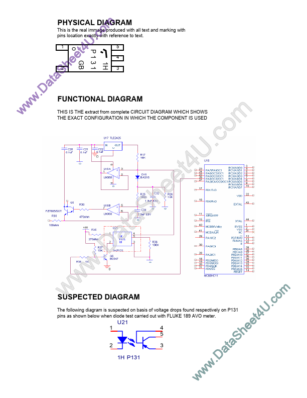
PHYSICAL DIAGRAM This is the real immage produced with all text and marking with pins location exactly with reference to text. 1 w w at .D FUNCTIONAL DIAGRAM w THIS IS THE extract from complete CIRCUIT DIAGRAM WHICH SHOWS THE EXACT CONFIGURATION IN WHICH THE COMPONENT IS USED aS 2 e e h U 4 t m o .c 1H 5 4 3 P131 SUSPECTED DIAGRAM The following diagram is suspected on basis of voltage drops found respectively on P131 pins as shown below when diode test carried out with FLUKE 189 AVO meter. w w GB .D w 1 2 t a S a e h t e U 4 .c m o U21 4 5 3 1H P131 w w w .D a S a t e e h U 4 t m o .c