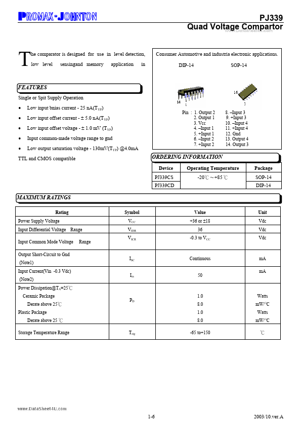
PJ339CD
PJ339CD is Quad Voltage Compartor manufactured by Unknown Manufacturer.
- Part of the PJ339 comparator family.
FEATURES
Single or Spit Supply Operation Low input bnias current
- 25 n A(TYP) Low input offset current
- ± 5.0 n A(TYP) Low input offset voltage
- ± 1.0 m V (TYP) Input mon-made voltage range to gnd Low output saturation voltage
- 130m V(TYP) @4.0m A
Pin : 1. Output 2 2. Output 1 3. Vcc 4.
- Input 1 5. +Input 1 6.
- Input 2 7. +Input 2 8.
- Input 3 9. +Input 3 10.
- Input 4 11. +Input 4 12. Gnd 13. Output 4 14. Output 3
TTL and CMOS patible
ORDERING INFORMATION
Device PJ339CS PJ339CD Operating Temperature -20℃〜+85 ℃ Package SOP-14 DIP-14
MAXIMUM RATINGS
Rating Power Supply Voltage Input Differential Voltage Range Range Symbol VCC VIDR VICR Value +36 or ±18 36 -0.3 to VCC Unit Vdc Vdc Vdc
Input mon Mode Voltage Output Short-Circuit to Gnd (Note1) Input Current(Vin -0.3 Vdc) (Note2) Power Dissipation@TA=25℃ Ceramic Package Derate above 25℃ Plastic Package Derate above 25 ℃ Storage Temperature Range
ISC Iin
Continuous m A m A
1.0 8.0 1.0 8.0
Watts m W/ΟC Watts m W/ΟC
Tstg
-65 to+150
℃
1-6
2003/10.ver.A
PJ339 Quad Voltage partor ..
ELECTRICAL CHARACTERISTICS (VCC= 5.0Vdc,TA= 25 ℃ unless otherwise noted.)
Characteristics Input offset voltage (Note 3) Input Bias Current (Note 3,4) (Output in Linear Range) Input Offset Current (Note 3) Input mon-Mode Voltage Range (Note 6) Supply Current RL = ∞ (For All parators) RL = ∞ , VCC =30Vdc Voltage Gain RL ≥ 15KΩ , VCC = 15Vdc Large Signal Response Time V1 = TTL logic Swing, Vref = 1.4 Vdc, VRL = 5.0Vdc, RL = 5.1 KΩ Response Time (Note 6) VRL = 5.0 Vdc, RL =5.1 KΩ Output Sink Current VI(-) ≥ +1.0 Vdc, VI(+) = 0, VO≤15Vdc Saturation Voltage VI(-) ≥ +1.0 Vdc, VI (+) = 0, Isink ≤ 4.0 m A Output Leakage Current VI(+) ≥ +1.0 Vdc, VI(-) = 0, VO =+5.0Vdc Input Offset Voltage (Note 3) TA = -20℃ to +85℃ Input Bias Current (Note 3 4) (Output in Linear Range) TA = -20 ℃ to +85 ℃ Input Offset Current (Note 3) TA = -20 ℃ to +85 ℃ Input mon-Mode Voltage Range TA = -20 ℃ to +85 ℃ Saturation Voltage VI(-) ≥ + 1.0 Vdc, VI (+) = 0, Isink...