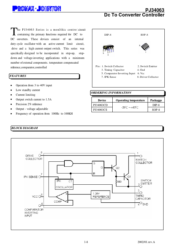
• Part: PJ34063
  • Description: Dc To Converter Controller
  • Manufacturer: Unknown Manufacturer
  • Size: 338.90 KB
Download PJ34063 Datasheet PDF
Unknown Manufacturer
PJ34063
PJ34063 is Dc To Converter Controller manufactured by Unknown Manufacturer.
FEATURES - - - Operation from 3 to 40V input Low standby current Current limiting Output switch current to 1.5A Precision 2% reference Output - voltage adjustable Frequency of operation from 100Hz to 100KH ORDERING INFORMATION Device PJ34063CD PJ34063CS Operating temperature -20℃~+85℃ Packagge DIP-8 SOP-8 - - - - BLOCK DIAGRAM 1-8 2002/01. rev.A PJ34063 Dc To Converter Controller ABSOLUTE MAXIMUM RATINGS Characte ristic Power Supply Voltage parator Input Voltage Range Switch Collector Voltage Switch Emitter Voltage Switch Collector to Emitter Voltage Driver Collector Voltage Drive Collector Current (Note 1) Switch Current Operating Junction Temperature Operating Ambient Temperature Range Storage Temperature Range Symbol VCC VIR VC(SW) VE(SW) VCE(SW) VC(drive) IC(drive) Isw TJ TA Tstg Value 40 -0.3 ~ +40 40 40 40 40 100 1.5 +150 -20 to +85 -65 to +150 Unit Vdc Vdc Vdc Vdc Vdc Vdc m A A ℃ ℃ ℃ ELECTRICAL CHARACTERISTICS (VCC = 5.0V. Ta= Tlow to Thigh. unless otherwise specified) Characte ristic OSCILLATOR Frequency Charging Current Discharge Current Discharge To Charge Current Ratio Current Limit Sense Voltage OUTPUT SWITCH(NOTE 2) Saturation Voltage , Darlington Connection Saturation Voltage , Darlington Connection DC Current Gain Collector Off- State Current PARATOR Threshold Voltage Threshold Voltage Line Regulation Input Bias Current TOTAL DEVICE Supply Current Symbol fosc Ichg Idischg Idischg/ Ichg VIPK(sense) VCE(sat) VCE(sat) h FE IC(off) VTH Regline IIB ICC Te st Condition VPIN5=0V, C T =1.0n F , T A=25℃ VCC=5 to 40V, T A=25℃ VCC=5 to 40V, T A=25℃ Pin7 to VCC , T A=25℃ Ichg = Idischg, T A=25℃ Isw=1.0A, Pins1,8 connected Isw=1.0A, R PIN8=82Ω to Vcc, Forced β≌20 Isw=1.0A, VCE = 5.0V, T A=25℃ VCE =40V T A=25℃ VCC = 3 to 40V VIN=0V VCC=5 to 40V, C T =1.0n F, Pin7=Vcc ,VPIN 5>Vth Pin 2 =GND, remaining pins open Min 24 24 140 5.2 250 50 1.23 Typ 33 35 220 6.5 300 1.0 0.45 75 40 1.25 1.4 -20 Max 42 42 260 7.5 350 1.3 0.7 100 1.27 5.0 -400 4.0 Unit KHz μA...