Datasheet4U Logo Datasheet4U.com

PLL500-17 - Low Phase Noise VCXO (17MHz to 36MHz)

General Description

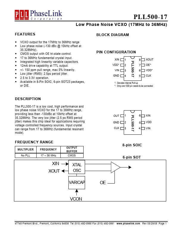
The PLL500-17 is a low cost, high performance and low phase noise VCXO for the 17 to 36MHz range, providing less than -130dBc at 10kHz offset at 35.328MHz.

The very low jitter (2.5 ps RMS period jitter) makes this chip ideal for applications requiring voltage controlled frequency sources.

Key Features

  • VCXO output for the 17MHz to 36MHz range Low phase noise (-130 dBc @ 10kHz offset at 35.328MHz). CMOS output with OE tri-state control. 17 to 36MHz fundamental crystal input. Integrated high linearity variable capacitors. 12mA drive capability at TTL output. +/- 150 ppm pull range, max 5% linearity. Low jitter (RMS): 2.5ps period jitter. 2.5 to 3.3V operation. Available in 8-Pin SOIC, 6-pin SOT23.

📥 Download Datasheet

Datasheet Details

Part number PLL500-17
Manufacturer Unknown Manufacturer
File Size 215.35 KB
Description Low Phase Noise VCXO (17MHz to 36MHz)
Datasheet download datasheet PLL500-17 Datasheet

Full PDF Text Transcription (Reference)

The following content is an automatically extracted verbatim text from the original manufacturer datasheet and is provided for reference purposes only.

View original datasheet text
PLL500-17 Low Phase Noise VCXO (17MHz to 36MHz) FEATURES • • • • • • • • • • VCXO output for the 17MHz to 36MHz range Low phase noise (-130 dBc @ 10kHz offset at 35.328MHz). CMOS output with OE tri-state control. 17 to 36MHz fundamental crystal input. Integrated high linearity variable capacitors. 12mA drive capability at TTL output. +/- 150 ppm pull range, max 5% linearity. Low jitter (RMS): 2.5ps period jitter. 2.5 to 3.3V operation. Available in 8-Pin SOIC, 6-pin SOT23 packages, or DIE.