SDM4953 Datasheet Text
S DM4953
J ul 06 2005 ver1.2
Dual P -C hannel E nhancement Mode Field E ffect Transistor
P R ODUC T S UMMAR Y
VDS S -30V
ID -4.6A
R DS (ON) ( m W ) Max
53 @ VGS = -10V 95 @ VGS =
- 4.5V
F E AT UR E S S uper high dense cell design for low R DS(ON).
R ugged and reliable. S urface Mount P ackage.
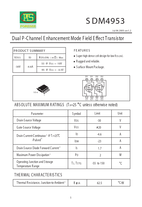
D1 D1 D2 D2
87 65
S O-8
1
1234
S1 G1 S2 G2
ABS OLUTE MAXIMUM R ATINGS (TA=25 C unless otherwise noted)
P arameter Drain-S ource Voltage Gate-S ource Voltage
Drain C urrent-C ontinuous a @ TJ=25 C -P ulsed b
Drain-S ource Diode Forward C urrent a Maximum P ower Dissipation a Operating Junction and S torage Temperature R ange
S ymbol VDS VGS ID IDM IS PD
TJ, TSTG
Limit -30 20 -4.6 -23 1.7 2
-55 to 150
Unit V V A A A W
C
THE R MAL CHAR ACTE R IS TICS
Thermal R esistance, Junction-to-Ambient a
R JA...