SMW200-26C
SMW200-26C is 2.00mm PITCH CONNECTOR manufactured by Unknown Manufacturer.
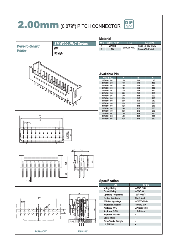
- Part of the SMW200-10C comparator family.
- Part of the SMW200-10C comparator family.
DESCRIPTION
The 2SK3324 is N-Channel MOS FET device that features a Low gate charge and excellent switching characteristics, and Designed for high voltage applications such as switching power supply, AC adapter.
ORDERING INFORMATION
PART NUMBER 2SK3324 PACKAGE TO-3P
FEATURES
- Low gate charge : QG = 32 n C TYP. (VDD = 450 V, VGS = 10 V, ID = 6.0 A)
- Gate voltage rating : ±30 V
- Low on-state resistance : RDS(on) = 2.8 Ω MAX. (VGS = 10 V, ID = 3.0 A)
- Avalanche capability ratings (TO-3P)
ABSOLUTE MAXIMUM RATINGS (TA = 25 °C)
Drain to Source Voltage Gate to Source Voltage Drain Current (DC) Drain Current (Pulse)
Note1
VDSS VGSS(AC) ID(DC) ID(pulse) PT PT Tstg
Note2 Note2
900 ±30 ±6 ±18 120 3.0
- 55 to + 150 6.0 21.6
V V A A W W °C A m J
Total Power Dissipation (TC = 25°C) Total Power Dissipation (TA = 25°C) Storage Temperature Single Avalanche Current Single Avalanche Energy
IAS EAS
Notes 1. PW ≤ 10 µs, Duty cycle ≤ 1 % 2. Starting Tch = 25 °C, VDD = 150 V, RG = 25 Ω, VGS = 20 V → 0 V
The information in this document is subject to change without notice. Before using this document, please confirm that this is the latest version.
Not all devices/types available in every country. Please check with local NEC representative for availability and additional information.
Document No. D14203EJ2V0DS00 (2nd edition) Date Published January 2000 NS CP(K) Printed in Japan
The mark
- shows major revised points.
©
Free Datasheet http://..
2SK3324
ELECTRICAL CHARACTERISTICS (TA = 25 °C)
CHARACTERISTICS Drain Leakage Current Gate to Source Leakage Current Gate to Source Cut-off Voltage SYMBOL IDSS IGSS VGS(off) | yfs | RDS(on) Ciss Coss Crss td(on) tr td(off) tf QG QGS QGD VF(S-D) trr Qrr 2.5 2.5 3.3 2.5 1000 200 42 17 38 57 33 32 5 20 0.9 1.9 9.0 2.8 MIN. TYP. MAX. 100 ±100 3.5 UNIT TEST CONDITIONS VDS = 900 V, VGS = 0 V VGS = ±30 V, VDS = 0 V VDS = 10 V, ID = 1.0 m A VDS = 20 V, ID = 3.0 A VGS = 10 V, ID = 3.0 A VDS = 10 V, VGS = 0 V, f = 1 MHz VDD = 150 V, ID =...