Datasheet Details
| Part number | TS08N02S |
|---|---|
| Manufacturer | Unknown Manufacturer |
| File Size | 832.63 KB |
| Description | Single N-Channel Power MOSFET |
| Datasheet | TS08N02S-ETC.pdf |
|
|
|
Overview: TS08N02S Single N-Channel Power MOSFET VDSS(V) 20 RDS (ON) 8mΩ(Typ)@VGS=4.5V 11.7mΩ(Typ)@VGS=2.5V ID(A) 12 FEATURE: • The TS08N02S is the high cell density trenched N-ch MOSFETS, which provides excellent RDSON and efficiency for most of the small power switching and load switch applications.
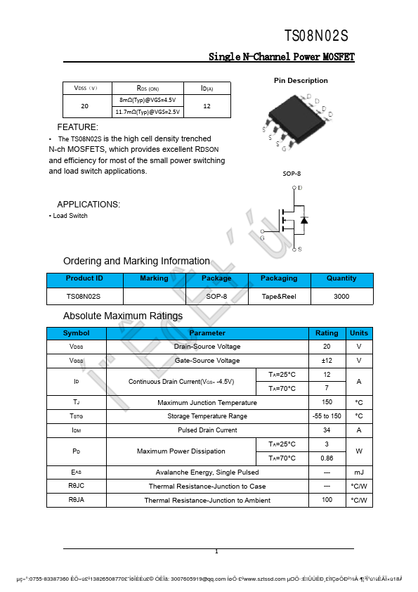
| Part number | TS08N02S |
|---|---|
| Manufacturer | Unknown Manufacturer |
| File Size | 832.63 KB |
| Description | Single N-Channel Power MOSFET |
| Datasheet | TS08N02S-ETC.pdf |
|
|
|
SOP-8 APPLICATIONS: ͨʢʱ´ú •LoadSwitch Ordering and Marking Information Product ID Marking Package Packaging TS08N02S SOP-8 Tape&Reel Absolute Maximum Ratings Symbol VDSS VGSS ID TJ Parameter Drain-Source Voltage Gate-Source Voltage Continuous Drain Current(VGS= -4.5V) Maximum Junction Temperature TA=25°C TA=70°C TSTG Storage Temperature Range IDM Pulsed Drain Current TA=25°C PD Maximum Power Dissipation TA=70°C EAS Avalanche Energy, Single Pulsed RθJC Thermal Resistance-Junction to Case RθJA Thermal Resistance-Junction to Ambient Quantity 3000 Rating Units 20 V ±12 V 12 A 7 150 °C -55 to 150 °C 34 A 3 W 0.86 --- mJ --- °C/W 100 °C/W 1 µç»°:0755-83387360 ÊÖ»ú£º13826508770£¨ÍõÏÈÉú£© ÓÊÏä: 3007605919@qq.
꿅᣼.sztssd.
µØÖ·:ÉîÛÚÊи£ÌïÇøÖк½Â·¶¦³Ï¹ú¼ÊÄÏ×ù18Â¥1814 TS08N02S Single N-Channel Power MOSFET Electrical Characteristics (TA=25°C Unless Otherwise Noted) Symbo l Parameter Static Characteristics BVDSS Drain-Source Breakdown Voltage VGS(th) Gate threshold voltage RDS(ON) Drain-Source On-state Resistance IGSS Gate-source leakage current IDSS Zero gate voltage drain current Dynamic Characteristic Ciss Input Capacitance Coss Output Capacitance Crss Reverse Transfer Capacitance QG Gate Total Charge Qgs Gate-Source charge Qgd Gate-Drain charge td(on) Turn-on delay time tr Turn-on Rise Time td(off) Turn-off Delay Time tf Turn-off Fall Time RG Gate Resistance Diode Characteristics VSD Diode Forward Voltage trr Reverse Recovery Time Qrr Reverse Recovery Charge Conditions Min.
| Part Number | Description |
|---|