UC3715
UC3715 is Complementary Switch FET Drivers manufactured by Unknown Manufacturer.
- Part of the UC3714 comparator family.
- Part of the UC3714 comparator family.
DESCRIPTION
These two families of high speed drivers are designed to provide drive waveforms for plementary switches. plementary switch configurations are monly used in synchronous rectification circuits and active clamp/reset circuits, which can provide zero voltage switching. In order to facilitate the soft switching transitions, independently programmable delays between the two output waveforms are provided on these drivers. The delay pins also have true zero voltage sensing capability which allows immediate activation of the corresponding switch when zero voltage is applied. These devices require a PWM-type input to operate and can be interfaced with monly available PWM controllers. In the UC3714 series, the AUX output is inverted to allow driving a p-channel MOSFET. In the UC3715- series the two outputs are configured in a true plementary fashion.
- The UC3715 series are not produced yet.
FEATURES
- Single Input (PWM and TTL patible)
- High Current Power FET Driver, 1.0A Source/2A Sink
- Auxiliary Output FET Driver, 0.5A Source/1A Sink
- Time Delays Between Power and Auxiliary Outputs Independently Programmable from 50ns to 500 ns
- Time Delay or True Zero-Voltage Operation Independently Configurable for Each Output
- Switching Frequency to 1MHz
- Typical 50 ns Propagation Delays
- ENBL Pin Activates 220 µA Sleep Mode
- Power Output is Active Low in Sleep Mode
- Synchronous Rectifier Driver
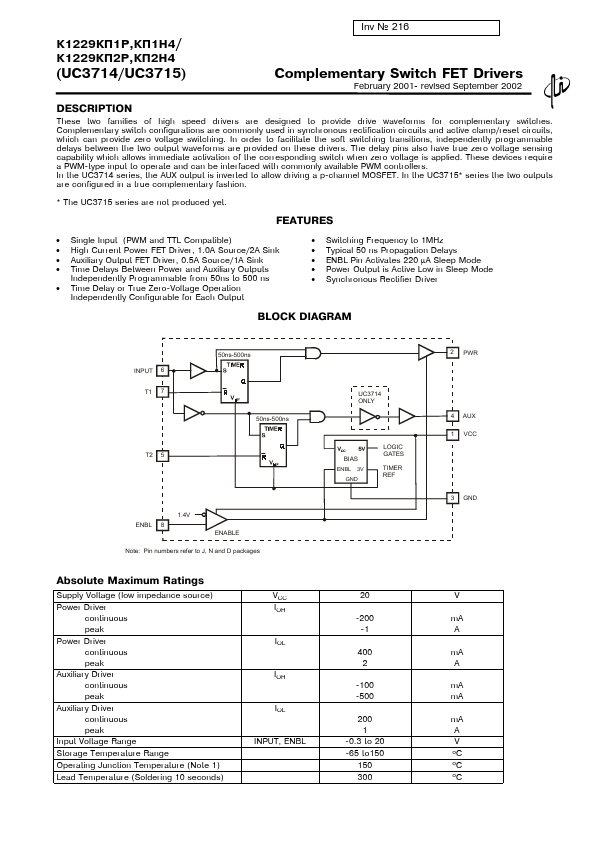
BLOCK DIAGRAM
INPUT 6 T1 7
T2 5
50ns-500ns 50ns-500ns
UC3714 ONLY
BIAS ENBL 3V
LOGIC GATES
TIMER REF
ENBL 8
1.4V
ENABLE
Note: Pin numbers refer to J, N and D packages
Absolute Maximum Ratings
Supply Voltage (low impedance source) Power Driver continuous peak Power Driver continuous peak Auxiliary Driver continuous peak Auxiliary Driver continuous peak Input Voltage Range Storage Temperature Range Operating Junction Temperature (Note 1) Lead Temperature (Soldering 10 seconds)
VCC IOH
INPUT, ENBL
-200 -1
400 2
-100 -500
200 1
-0.3 to 20 -65...