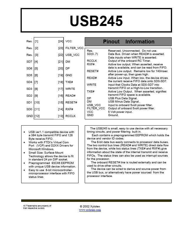
Click to expand full text
USB245
Res. [1] Res. [2] Res. [3] SD7 [4] SD6 [5] SD5 [6] SD4 [7] SD3 [8] SD2 [9] SD1 [10] SD0 [11] GND [12] [24] VCC [23] FILTER_VCC [22] USB_VCC [21] DM [20] DP [19] GND [18] TXE# [17] WRITE [16] READ# [15] RESET# [14] RXF# [13] RCCLK Res. SD(0..7) RCCLK RXF# RESET# READ# WRITE TXE# DP DM USB_VCC FILTER_VCC VCC GND
Pinout
Information
Reserved, Unconnected. Do not use. Data Bus. Driven when READ# is asserted. Data inputs when WRITE is asserted. Output of the onboard RC Timer. Active low output. When asserted, receive data is available, and can be read from FIFO. Active Low output. Remains low for 140msec after power-up, then goes high. Active Low input. When low, the device drives the current receive FIFO data onto SD0-SD7.