FEATURES
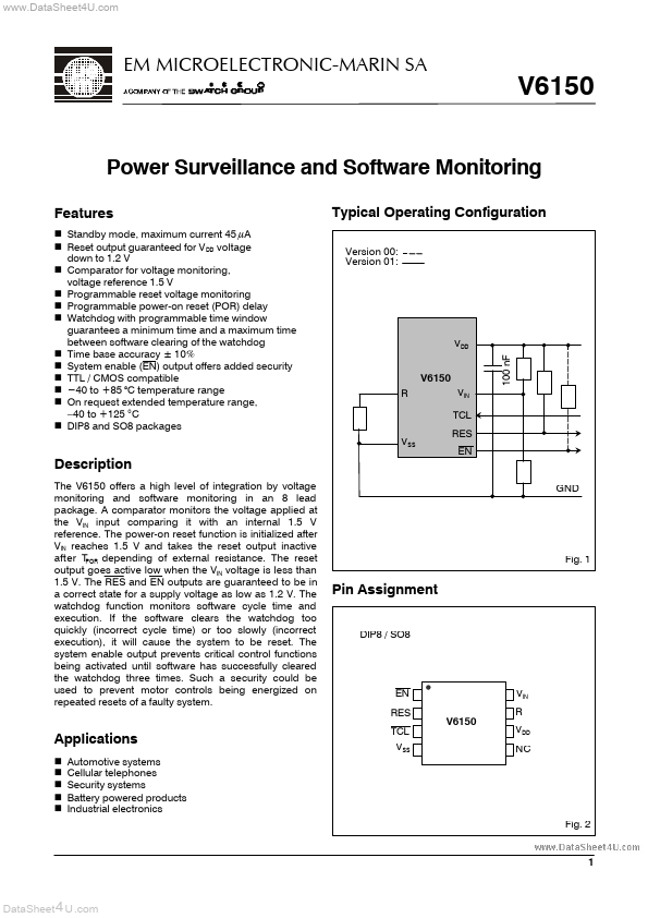
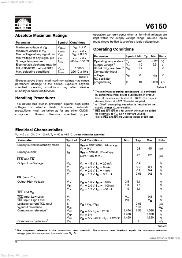
n Standby mode, maximum current 45 mA n Reset output guaranteed for V DD voltage down to 1.2 V n Comparator for voltage monitoring, voltage reference 1.5 V n Programmable reset voltage monitoring n Programmable power-on reset (POR) delay n Watchdog with programmable time window guarantees a minimum time and a maximum time between software clearing of the watchdog n Time base accuracy ± 10% n System enable (EN) output offers added security n TTL / CMOS compatible n -40 to +85 °C temperature range n On request extended temperature range, −40 to +125 ° C n DIP8 and SO8 packages Typical Operating Configuration Version 00: Version 01: VDD V6150 R VIN TCL VSS RES EN GND 100 nF DESCRIPTION
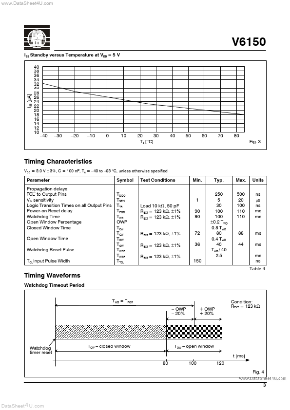
A comparator monitors the voltage applied at the VIN input comparing it with an internal 1.5 V reference. The RES and EN outputs are guaranteed to be in a correct state for a supply voltage as low as 1.2 V. The watchdog function monitors software cycle time and execution. If the software clears the watchdog too quickly (incorrect cycle time) or too slowly (incorrect execution), it will cause the system to be reset.