VDSGLD38.88
VDSGLD38.88 is Voltage Controlled Crystal Oscillator manufactured by Unknown Manufacturer.
Product Data Sheet
VDSGLD @ 38.88 MHz
Voltage Controlled Crystal Oscillator
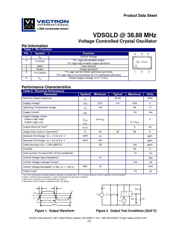
Pin Information
Table 1. Pin Function Pin Symbol
1 2 3 4 5 6 VC Tri-State GND Output TTL/CMOS Vcc
Function
Control Voltage TTL logic low disables output TTL logic high enables output waveform Case Ground Output waveform TTL logic low for CMOS optimized symmetry TTL logic high or no connection for TTL optimized symmetry Power Supply Voltage (3.3 V ±10%)
Performance Characteristics
Table 2. Electrical Performance Parameter
Nominal Output Frequency Supply Voltage
Symbol f0 VDD TO IDD VOH VOL TR/TF
Minimum
2.97 -40
Typical
38.88 3.3
Maximum
3.63 85 20
Units
MHz V °C mA V
Operating Temperature Range Supply...