sda12
sda12 is SCHOTTKY DIODE ARRAY manufactured by Unknown Manufacturer.
DESCRIPTION
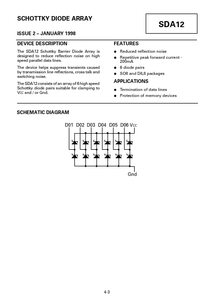
The SDA12 Schottky Barrier Diode Array is designed to reduce reflection noise on high speed parallel data lines. The device helps suppress transients caused by transmission line reflections, cross talk and switching noise. The SDA12 consists of an array of 6 high speed Schottky diode pairs suitable for clamping to VCC and / or Gnd.
FEATURES
- -
- -
- -
Reduced reflection noise Repetitive peak forward current 200m A 6 diode pairs SO8 and DIL8 packages
APPLICATIONS
Termination of data lines Protection of memory devices
SCHEMATIC DIAGRAM
D01 D02 D03 D04 D05 D06 VCC
Gnd
4-3
ABSOLUTE MAXIMUM RATING (at Tamb=25°C unless otherwise stated)-
Steady-State Reverse Voltage Continuous Forward Current Repetitive Peak Forward Current (3) Continuous Total Power Dissipation (4) (SO or DIL packages) Operating Free-air Temperature Range Storage Temperature Range 7V 50m A(1) 170m A(2)
200m A(1) 1A(2)
625m W 0 to 70°C -65 to 150°C
- Stresses beyond those listed above may cause permanent damage to the device. These are stress ratings only and functional operation of the device at these or any other conditions beyond those indicated under the remended operating conditions is not implied. Exposure to absolute maximum rated conditions for extended periods of time may affect device reliability. Note: (1) Any D terminal from Gnd or to VCC (2) Total through all Gnd or VCC terminals (3) These values apply for t W=100µs, duty cycle ≤ 20% (4) For operation above 25°C , derate linearly at the rate of 6.25m W/°C
ELECTRICAL CHARACTERISTICS (at Tamb=25°C unless otherwise stated) Single-Diode Operation
PARAMETER Static Forward Voltage SYMBOL VF
MIN. TYP. MAX. UNIT
CONDITIONS To VCC , IF=18m A To VCC , IF=50m A From Gnd, IF=18m A From Gnd, IF=50m A IF=200m A To VCC ,VR=7V From Gnd, VR=7V VR=0, f=1MHz VR=2V, f=1MHz
0.85 1.05 0.75 0.95
1.05 1.3 0.95 1.2 6 5
V V V V V µA µA p F p F
Peak Forward Voltage Static Reverse Current
VFM IR CT
Total Capacitance
6 4
16 6
Note:...