MC74VHC1GU04
MC74VHC1GU04 is Unbuffered Inverter manufactured by ETL.
Unbuffered Inverter
The MC74VHC1GU04 is an advanced high speed CMOS Unbuffered inverter fabricated with silicon gate CMOS technology. It achieves high speed operation similar to equivalent Bipolar Schottky TTL while maintaining CMOS low power dissipation. This device consists of a single unbuffered inverter. In bination with others, or in the MC74VHCU04 Hex Unbuffered Inverter, these devices are well suited for use as oscillators, pulse shapers, and in many other applications requiring a high- input impedance amplifier. For digital applications, the MC74VHC1G04 or the MC74VHC04 are remended. The internal circuit is posed of three stages, including a buffer output which provides high noise immunity and stable output. The MC74VHC1GU04 input structure provides protection when voltages up to 7 V are applied, regardless of the supply voltage. This allows the MC74VHC1GU04 to be used to interface 5 V circuits to 3 V circuits.
- High Speed: t PD = 2.5 ns (Typ) at V CC = 5 V
- Low Power Dissipation: I CC = 2 m A (Max) at T A = 25°C
- Power Down Protection Provided on Inputs
- Balanced Propagation Delays
- Pin and Function patible with Other Standard Logic Families
- Chip plexity: FETs = 105; Equivalent Gates = 26
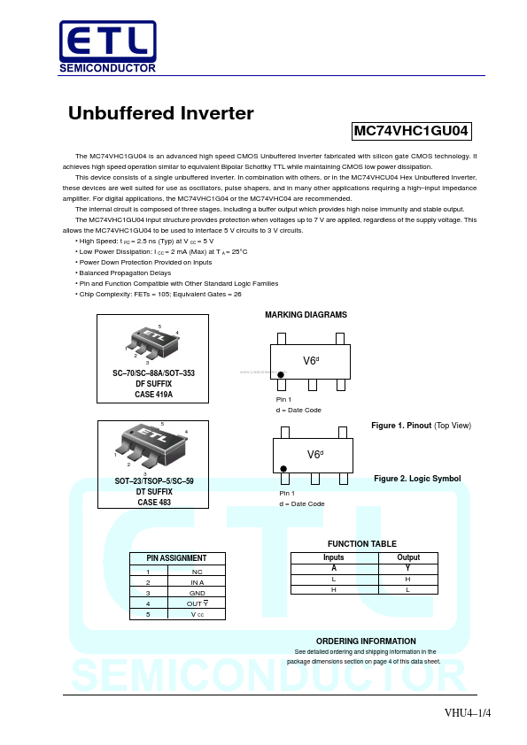
MARKING DIAGRAMS
5 4 1 2 3
V6d
..
SC- 70/SC- 88A/SOT- 353 DF SUFFIX CASE 419A
Pin 1 d = Date Code
5 4
Figure 1. Pinout (Top View)
1 2 3
V6d
Figure 2. Logic Symbol
Pin 1 d = Date Code
SOT- 23/TSOP- 5/SC- 59 DT SUFFIX CASE 483
FUNCTION TABLE
PIN ASSIGNMENT 1 2 3 4 5 NC IN A GND OUT Y V CC Inputs A L H Output Y H L
ORDERING INFORMATION
See detailed ordering and shipping information in the package dimensions section on page 4 of this data sheet.
VHU4- 1/4
MAXIMUM RATINGS
Value Unit
- 0.5 to + 7.0 V
- 0.5 to +7.0 V V CC=0
- 0.5 to +7.0 V High or Low State
- 0.5 to V cc + 0.5 I IK Input Diode Current
- 20 m A I OK Output Diode Current V OUT < GND; V OUT > V CC +20 m A I OUT DC Output Current, per Pin + 25 m A I CC DC Supply Current, V CC and GND...