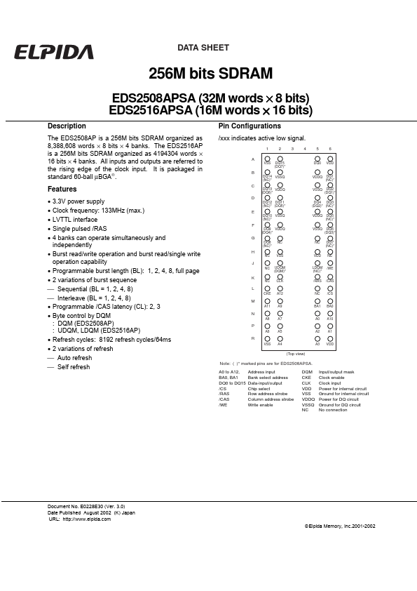
Datasheet4U Logo Datasheet4U.com

EDS2516APSA - 256M bits SDRAM

Description

The EDS2508AP is a 256M bits SDRAM organized as 8,388,608 words × 8 bits × 4 banks.

The EDS2516AP is a 256M bits SDRAM organized as 4194304 words × 16 bits × 4 banks.

All inputs and outputs are referred to the rising edge of the clock input.

Features

  • r>.
  • 3.3V power supply Clock frequency: 133MHz (max. ) LVTTL interface Single pulsed /RAS 4 banks can operate simultaneously and independently.
  • Burst read/write operation and burst read/single write operation capability.
  • Programmable burst length (BL): 1, 2, 4, 8, full page.
  • 2 variations of burst sequence  Sequential (BL = 1, 2, 4, 8)  Interleave (BL = 1, 2, 4, 8).
  • Programmable /CAS latency (CL): 2, 3.
  • Byte cont.

📥 Download Datasheet

Datasheet preview – EDS2516APSA

Datasheet Details

Part number EDS2516APSA
Manufacturer Elpida Memory
File Size 554.71 KB
Description 256M bits SDRAM
Datasheet download datasheet EDS2516APSA Datasheet
Additional preview pages of the EDS2516APSA datasheet.
Other Datasheets by Elpida Memory

Full PDF Text Transcription

Click to expand full text
DATA SHEET 256M bits SDRAM EDS2508APSA (32M words × 8 bits) EDS2516APSA (16M words × 16 bits) Description The EDS2508AP is a 256M bits SDRAM organized as 8,388,608 words × 8 bits × 4 banks. The EDS2516AP is a 256M bits SDRAM organized as 4194304 words × 16 bits × 4 banks. All inputs and outputs are referred to the rising edge of the clock input. It is packaged in standard 60-ball µBGA. Pin Configurations /xxx indicates active low signal. 1 A VSS DQ15 (DQ7)* DQ0 VDD 2 3 4 5 6 B DQ14 VSSQ (NC)* VDDQ DQ1 (NC)* DQ2 (DQ1)* Features • • • • • 3.3V power supply Clock frequency: 133MHz (max.
Published: |