EDS6432AFTA
EDS6432AFTA is 64M bits SDRAM manufactured by Elpida Memory.
Description
The EDS6432AFTA, EDS6432CFTA are 64M bits SDRAMs organized as 524,288 words × 32 bits × 4 banks. All inputs and outputs are synchronized with .. the positive edge of the clock. Supply voltages are 3.3V (EDS6432AFTA) and 2.5V (EDS6432CFTA). It is packaged in 86-pin plastic TSOP (II).
Pin Configurations
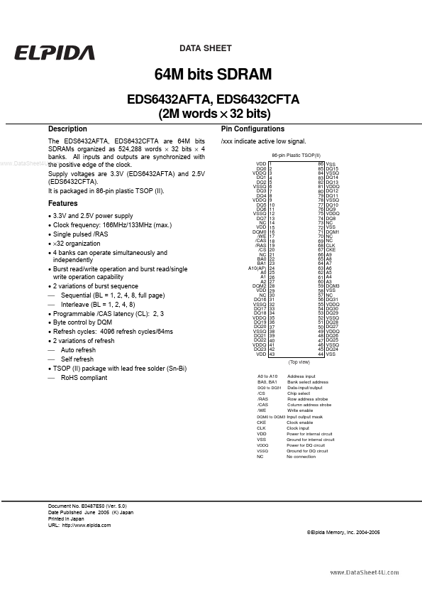
/xxx indicate active low signal.
86-pin Plastic TSOP(II)
Features
- -
- -
- 3.3V and 2.5V power supply Clock frequency: 166MHz/133MHz (max.) Single pulsed /RAS ×32 organization 4 banks can operate simultaneously and independently
- Burst read/write operation and burst read/single write operation capability
- 2 variations of burst sequence Sequential (BL = 1, 2, 4, 8, full page) Interleave (BL = 1, 2, 4, 8)
- Programmable /CAS latency (CL): 2, 3
- Byte control by DQM
- Refresh cycles: 4096 refresh cycles/64ms
- 2 variations of refresh Auto refresh Self refresh
- TSOP (II) package with lead free solder (Sn-Bi) Ro HS pliant
VDD DQ0 VDDQ DQ1 DQ2 VSSQ DQ3 DQ4 VDDQ DQ5 DQ6 VSSQ DQ7 NC VDD DQM0 /WE /CAS /RAS /CS NC BA0 BA1 A10(AP) A0 A1 A2 DQM2 VDD NC DQ16 VSSQ DQ17 DQ18 VDDQ DQ19 DQ20 VSSQ DQ21 DQ22 VDDQ DQ23 VDD
1 2 3 4 5 6 7 8 9 10 11 12 13 14 15 16 17 18 19 20 21 22 23 24 25 26 27 28 29 30 31 32 33 34 35 36 37 38 39 40 41 42 43
86 85 84 83 82 81 80 79 78 77 76 75 74 73 72 71 70 69 68 67 66 65 64 63 62 61 60 59 58 57 56 55 54 53 52 51 50 49 48 47 46 45 44
VSS DQ15 VSSQ DQ14 DQ13 VDDQ DQ12 DQ11 VSSQ DQ10 DQ9 VDDQ DQ8 NC VSS DQM1 NC NC CLK CKE A9 A8 A7 A6 A5 A4 A3 DQM3 VSS NC DQ31 VDDQ DQ30 DQ29 VSSQ DQ28 DQ27 VDDQ DQ26 DQ25 VSSQ DQ24 VSS
(Top view)
A0 to A10 BA0, BA1
DQ0 to DQ31
/CS /RAS /CAS /WE CKE CLK VDD VSS
VDDQ VSSQ
Address input Bank select address Data-input/output Chip select Row address strobe
Column address strobe
Write enable Clock enable Clock input
Power for internal circuit Ground for internal circuit Power for DQ circuit Ground for DQ circuit
DQM0 to DQM3 Input output mask
No connection
Document No. E0487E50 (Ver. 5.0)...