Datasheet4U Logo Datasheet4U.com

EM42BM3284LBA - Double DATA RATE SDRAM

General Description

The EM42BM3284LBA is Double-Date-Rate Synchronous DRAM fabricated with ultra high performance CMOS process containing 1,073,741,824 bits which organized as 8Meg words x 4 banks by 32 bits.

The 1Gb DDR SDRAM uses a double data rate architecture to accomplish high-speed operation.

Key Features

  • Internal Double-Date-Rate architecture with 2 Accesses per clock cycle.
  • 1.8V ±0.1V VDD/VDDQ.
  • 1.8V LV-COMS compatible I/O.
  • Burst Length (B/L) of 2, 4, 8, 16.
  • 3 Clock read latency.
  • Bi-directional,intermittent data strobe(DQS).
  • All inputs except data and DM are sampled at the positive edge of the system clock.
  • Data Mask (DM) for write data.
  • Sequential & Interleaved Burst type available.
  • Auto Precharge optio.

📥 Download Datasheet

Datasheet Details

Part number EM42BM3284LBA
Manufacturer Eorex
File Size 352.86 KB
Description Double DATA RATE SDRAM
Datasheet download datasheet EM42BM3284LBA Datasheet

Full PDF Text Transcription (Reference)

The following content is an automatically extracted verbatim text from the original manufacturer datasheet and is provided for reference purposes only.

View original datasheet text
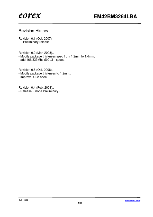
eorex EM42BM3284LBA Revision History Revision 0.1 (Oct. 2007) - Preliminary release. Revision 0.2 (Mar. 2008).. - Modify package thickness spec from 1.2mm to 1.4mm. - add 166/333Mhz @CL3 speed. Revision 0.3 (Oct. 2008).. - Modify package thickness to 1.2mm.. - Improve ICCs spec. Revision 0.4 (Feb. 2009).. - Release. ( none Preliminary) Feb. 2009 www.eorex.com 1/24 eorex EM42BM3284LBA 1Gb (8M×4Bank×32) Double DATA RATE SDRAM Features • Internal Double-Date-Rate architecture with 2 Accesses per clock cycle. • 1.8V ±0.1V VDD/VDDQ • 1.8V LV-COMS compatible I/O • Burst Length (B/L) of 2, 4, 8, 16 • 3 Clock read latency • Bi-directional,intermittent data strobe(DQS) • All inputs except data and DM are sampled at the positive edge of the system clock.