APM4532
APM4532 is Dual MOSFET manufactured by Unknown Manufacturer.
Features
- N-Channel 30V/5A, RDS(ON)=35mΩ(typ.) @ VGS=10V RDS(ON)=60mΩ(typ.) @ VGS=4.5V
Pin Description
S1 G1 S2 G2 1 2 3 4 8 7 6 5 D1 D1 D2 D2
- P-Channel -30V/-3.5A, RDS(ON)=85mΩ(typ.) @ VGS=-10V RDS(ON)=135mΩ(typ.) @ VGS=-4.5V
SO-8
- -
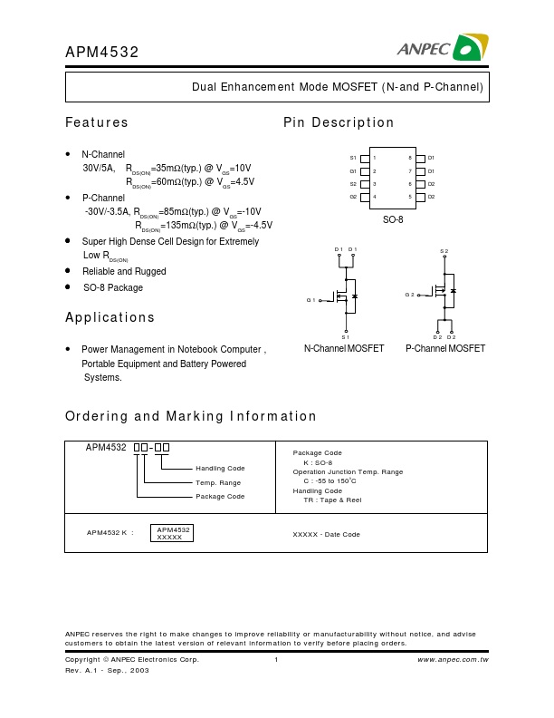
- Super High Dense Cell Design for Extremely Low RDS(ON) Reliable and Rugged SO-8 Package
G2 G1 D1 D1 S2
Applications
S1 D2 D2
- Power Management in Notebook puter , Portable Equipment and Battery Powered Systems.
N-Channel MOSFET
P-Channel MOSFET
Ordering and Marking Information
Handling Code Temp. Range Package Code Package Code K : SO-8 Operation Junction Temp. Range C : -55 to 150°C Handling Code TR : Tape & Reel
APM4532 K :
APM4532 XXXXX
XXXXX
- Date Code
ANPEC reserves the right to make changes to improve reliability or manufacturability without notice, and advise customers to obtain the latest version of relevant information to verify before placing orders. Copyright ANPEC Electronics Corp. Rev. A.1
- Sep., 2003 1 .anpec..tw
Absolute Maximum Ratings
Symbol VDSS VGSS ID
- (TA = 25°C unless otherwise noted)
N-Channel 30 ±25 5 20 P-Channel -30 ±25 -3.5 -20 2 0.8 150 -55 to 150 62.5 °C °C °C/W A V Unit
Parameter Drain-Source Voltage Gate-Source Voltage Maximum Drain Current
- Continuous Maximum Drain Current
- Pulsed TA=25°C Maximum Power Dissipation Maximum Junction Temperature Storage Temperature Range Thermal Resistance
- Junction to Ambient TA=100°C
IDM PD TJ TSTG Rθj A
2 0.8
- Surface Mounted on FR4 Board, t ≤ 10 sec.
Electrical Characteristics
Symbol Static BVDSS IDSS VGS(th) IGSS Drain-Source Breakdown Voltage Zero Gate Voltage Drain Current Gate Threshold Voltage Parameter
(TA = 25°C unless otherwise noted)
APM4532 Unit Min. Typ. Max. N-Ch P-Ch N-Ch P-Ch N-Ch P-Ch N-Ch P-Ch N-Ch P-Ch N-Ch P-Ch 35 60 85 135 0.7 -0.7 1 -1 1.5 -1.5 30 -30 1 -1 2 -2 ±100 ±100 45 70 95 150 1.3 -1.3 V mΩ n A
Test Condition
VGS=0V , IDS=250µA VDS=24V , VGS=0V VDS=-24V , VGS=0V VDS=VGS , IDS=250µA...