DESCRIPTION
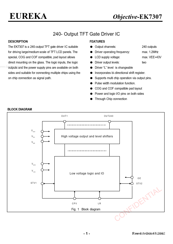
Supports multi chip operation via output pins. Pulse width modulation function. COG and COF compatible pad layout Power and logic I/O pins on both sides Through Chip connection 240 outputs max. 1.2MHz max. VEE+43V two outputs and the power supply pins are available on both sides and suitable for connecting multiple chips using the on chip connection as signal path. BLOCK DIAGRAM OUT1 OUT240 VGH VGL VEE High voltage output and level shifters VDD V SS Low voltage logic and IO OE STV1 STV2 CPV LR Fig. 1 Block diagram N O C N E D I F AL I T -1- Rev 0.1 Oct.17.2002 EUREKA PINNING INFORMATION Table 1. Pad description PAD Nr. 53 to 292 13 to 18, 327 to 332 7 t0 12, 333 to 338, 346 to 349, 467 to 470 31 to 33, 38 to 41, 304 to 307 312 to 314 25 to 27 318 to 320 28 to 30 315 to 317 34 to 37 308 to 311 42 to 45 300 to 303 1 to 6 339 to 344 350 to 355 461 to 466 19 to 24 321 to 326 356 to 361 455 to 460 SYMBOL OUT1 - OUT240 VGL VEE VSS LR STV1 STV2 CPV OE I/O Start pulse input and out...