ST49C107A-04
ST49C107A-04 is Preprogrammed CPU Mother Board Frequency Generator manufactured by Exar.
FEATURES
D Provides Reference Clock And Synthesized Clock D 5 to 32 MHz Input Reference Frequency D Pin-to-Pin patible to Avasem AV9107 D Programmable Analog Phase Locked Loop D Low Power Single 5V CMOS Technology D Up to 16 Frequencies Stored Internally D 8/14 pin DIP or SOIC Package
GENERAL DESCRIPTION
The ST49C107A-04 is a mask programmable monolithic analog CMOS device designed to generate two simultaneous clocks. The output frequency can vary from 2 to 130MHz, with up to 16 single selectable preprogrammed frequencies stored in internal ROM. The ST49C107A-04 is designed to replace existing CPU mother board clocks generated from individual oscillators ORDERING INFORMATION
Part No. ST49C107ACF14-04 Package 14 Lead 150 Mil JEDEC SOIC Operating Temperature Range 0°C to 70°C in order to reduce board space and number of oscillators. To provide high speed and low jitter clock, the parts utilize a high speed analog CMOS phase locked loop using 14.318 MHz system clock as the reference clock (note that reference clock can be changed to generate optional frequencies from a standard programmed device). The programmed clock outputs are selectable via four address lines.
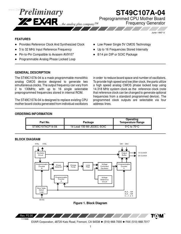
BLOCK DIAGRAM
XTAL XTAL OE1 OE2
Oscillator Circuit
Output Buffer
1X-CLOCK 2X-CLOCK
Programmable Counter B
Phase Detector
Charge Pump
Loop Filter
Voltage Controlled Oscillator
Programmable Counter C
Programmable Counter A
Voltage Reference Circuit
Rom Table Select Logic
B=5....128 A=5....128 C = 1, 2, 4
A0-A3
Figure 1. Block Diagram
Rev. P2.00
E1996
EXAR Corporation, 48720 Kato Road, Fremont, CA 94538 z (510) 668-7000 z FAX (510) 668-7017 1
PIN CONFIGURATION
Preliminary
A1 A2 A3 AGND DGND PD- XTAL1
1 2 3 4 5 6 7
14 13 12 11 10 9 8
A0 1XCLK VCC 2XCLK OE2 OE1 XTAL2
14 Lead SOIC (Jedec, 0.150”)
PIN DESCRIPTION
Symbol A1 A2 A3 AGND DGND PD XTAL1 Pin # 1 2 3 4 5 6 7 Type I I I O O I I Frequency Select Address Input 21 . Frequency Select Address Input 31. Frequency Select...