Exar Corporation XRK39653
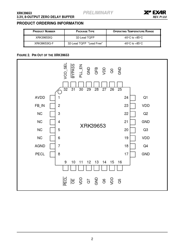
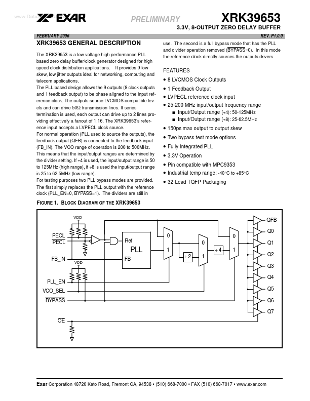
The XRK39653 is a low voltage high performance PLL based zero delay buffer/clock generator designed for high speed clock distribution applications. It provides 9 low skew, low jitter outputs ideal for networking, computing and telecom applications. The PLL based design allows the 9 outputs (8 clock outputs and 1 feedback output) to be phase aligned to the input reference clock.| Part No. | XRK39653 |
|---|---|
| Datasheet | XRK39653 Download |
| Manufacturer |  Exar Corporation |
| Description | 8-OUTPUT ZERO DELAY BUFFER |
| Buy | Stock & Price |
GENERAL DESCRIPTION
The outputs source LVCMOS compatible levels and can drive 50Ω transmission lines. If series termination is used, each output can drive up to 2 lines providing effectively a fanout of 1:16. The XRK39653’s reference input accepts a LVPECL clock source. For normal operation (PLL used to source the outputs), the feedback output (QFB) is connected to the feedback input (FB_IN). The VCO range of operation is 200 to 500MHz. This means that the input/output ranges are determined by the divider setting. If ÷4 is used, the input/output range is 50 to 125MHz (high range), if ÷8 is used the input/output range is 25 to 62.5MHz (low range). For testing purposes two PLL bypass modes are provided. The first simply replaces the PLL output with the reference clock (PLL_EN=0, BYPASS=1). The dividers are still inFEATURES
●●
●
● 8 LVCMOS Clock Outputs 1 Feedback Output LVPECL reference clock input 25-200 MHz input/output frequency range
● Input/Output range (÷4): 50-125MHz
● Input/Out...