FEATURES
FUNCTIONAL DESCRIPTION
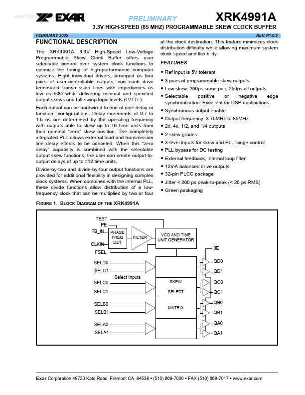
Eight individual drivers, arranged as four pairs of user-controllable outputs, can each drive terminated transmission lines with impedances as low as 50Ω while delivering minimal and specified output skews and full-swing logic levels (LVTTL). Delay increments of 0.7 to 1.5 ns are determined by the operating frequency with outputs able to skew up to ±6 time units from their nominal “zero” skew position. When this “zero delay” capability is combined with the selectable output skew functions, the user can create output-tooutput delays of up to ±12 time units. Divide-by-two and divide-by-four output functions are provided for additional flexibility in designing complex clock systems. When combined with the internal PLL, these divide functions allow distribution of a lowfrequency clock that can be multiplied by two or four FIGURE 1. BLOCK DIAGRAM OF THE XRK4991A TEST PE FB_IN PHASE CLKIN FSEL SELD0 SELD1 Select Inputs SELC0 SELC1 SELB0 SELB1 SELA0 SELA1 FREQ... Exar Corporation