GENERAL DESCRIPTION
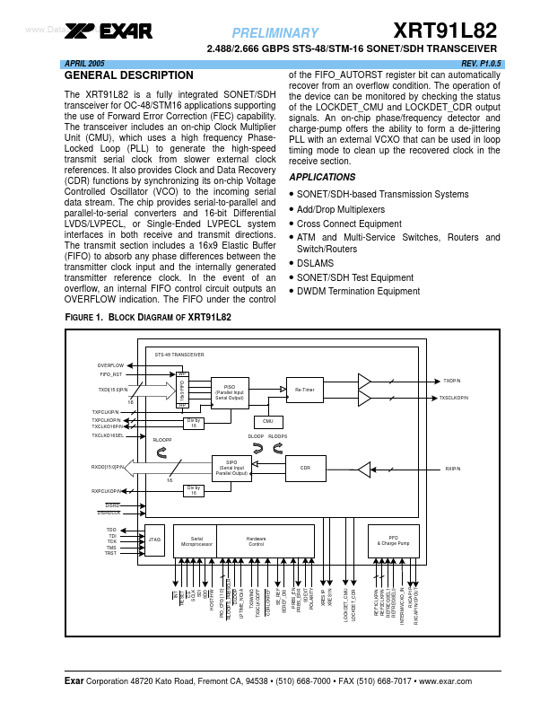
The chip provides serial-to-parallel and parallel-to-serial converters and 16-bit Differential LVDS/LVPECL, or Single-Ended LVPECL system interfaces in both receive and transmit directions. The transmit section includes a 16x9 Elastic Buffer (FIFO) to absorb any phase differences between the transmitter clock input and the internally generated transmitter reference clock. In the event of an overflow, an internal FIFO control circuit outputs an OVERFLOW indication. The FIFO under the control FIGURE 1. BLOCK DIAGRAM OF XRT91L82 of the FIFO_AUTORST register bit can automatically recover from an overflow condition. The operation of the device can be monitored by checking the status of the LOCKDET_CMU and LOCKDET_CDR output signals. An on-chip phase/frequency detector and charge-pump offers the ability to form a de-jittering PLL with an external VCXO that can be used in loop timing mode to clean up the recovered clock in the receive section. APPLICATIONS
● SONET/SDH-base... Exar Corporation