FEATURES
● Memory Protection - W# pin works in conjunction with Status Register Bits to protect specified memory areas - Status Register Block Protection Bits (BP2, BP1, BP0) in status register configure parts of memory as read only SOFTWARE FEATURES
● SPI Bus Compatible Serial Interface ES25P40 1 Rev. 0D May 11 , 2006 E ES S II ADVANCED INFORMATION Excel Semiconductor inc. GENERAL PRODUCT DESCRIPTION
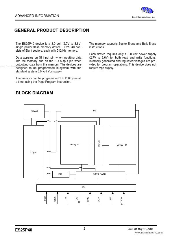
ES25P40 consists of Eight sectors, each with 512 Kb memory. Data appears on SI input pin when inputting data into the memory and on the SO output pin when outputting data from the memory. The memory supports Sector Erase and Bulk Erase instructions. Each device requires only a 3.0 volt power supply (2.7V to 3.6V) for both read and write functions. Internally generated and regulated voltages are provided for program operations. This device does not require Vpp supply. BLOCK DIAGRAM SRAM PS XDEC Array - L Logic Array - R RD DATA PATH IO CS# SCK SI GND HOLD# SO VCC W# ES25P40 2 Rev. 0D May 1... Excel Semiconductor