Excelliance MOS EMB07P03CS
P-Channel Logic Level Enhancement Mode Field Effect Transistor
| Part No. | EMB07P03CS |
|---|---|
| Datasheet | EMB07P03CS Download |
| Manufacturer |  Excelliance MOS |
| Description | P-Channel Logic Level Enhancement Mode Field Effect Transistor |
| Buy | Stock & Price |
ABSOLUTE MAXIMUM RATINGS
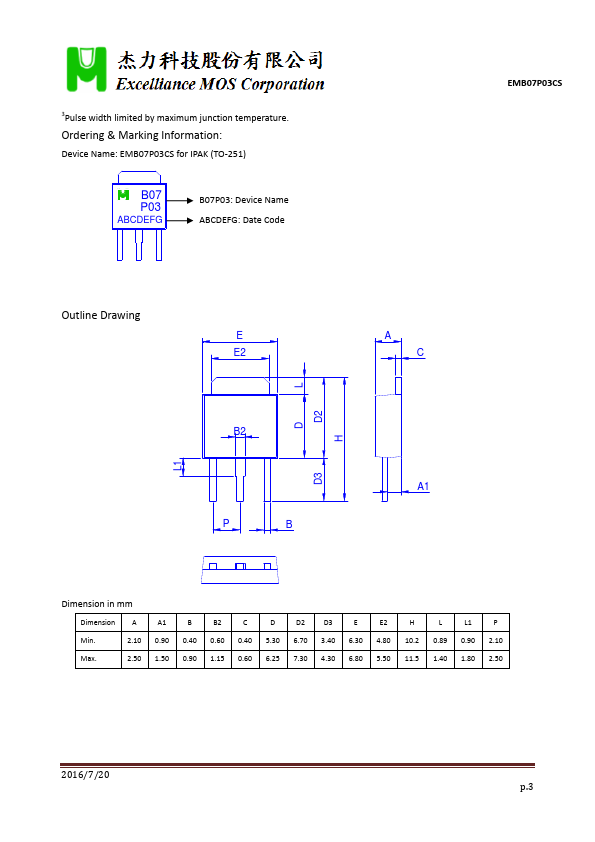
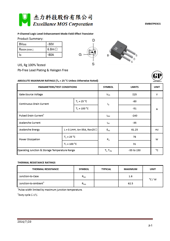
(TA = 25 °C Unless Otherwise Noted) PARAMETERS/TEST CONDITIONS SYMBOL Gate‐Source Voltage Continuous Drain Current Pulsed Drain Current1 TC = 25 °C TC = 100 °C Avalanche Current Avalanche Energy L = 0.1mH, ID=‐35A, RG=25Ω Power Dissipation TC = 25 °C TC = 100 °C Operating Junction & Storage Temperature Range VGS ID IDM IAS EAS PD Tj, Tstg THERMAL RESISTANCE RATINGS THERMAL RESISTANCE SYMBOL Junction‐to‐Case R●JC Junction‐to‐Ambient3 R●JA 1Pulse width limited by maximum junction temperature. 2Duty cycle 1% TYPICAL EMB07P03CS LIMITS ±25 ‐80 ‐51 ‐240 ‐35 61.25 78 31 ‐55 to 150 UNIT V A mJ W °C MAXIMUM 1.6 62.5 UNIT °C / W 2016/7/20 p.1 EMB07P03CSELECTRICAL CHARACTERISTICS
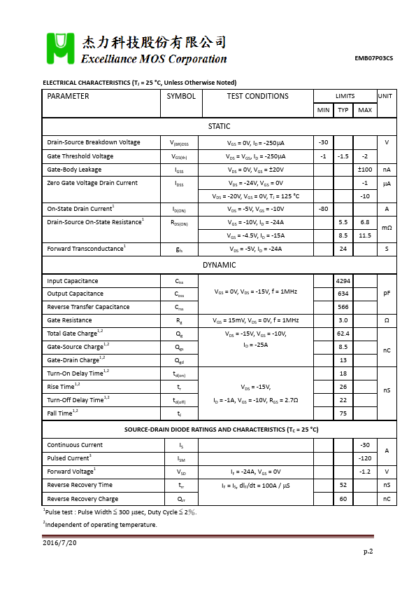
(TJ = 25 °C, Unless Otherwise Noted) PARAMETER SYMBOL TEST CONDITIONS LIMITS UNIT MIN TYP MAX STATIC Drain‐Source Breakdown Voltage Gate Threshold Voltage Gate‐Body Leakage Zero Gate Voltage Drain Current On‐State Drain Current1 Drain‐Source On‐State Resistance1 Forward Transconductance1 V(BR)...