EMB60N06J Overview
| Part | EMB60N06J |
|---|---|
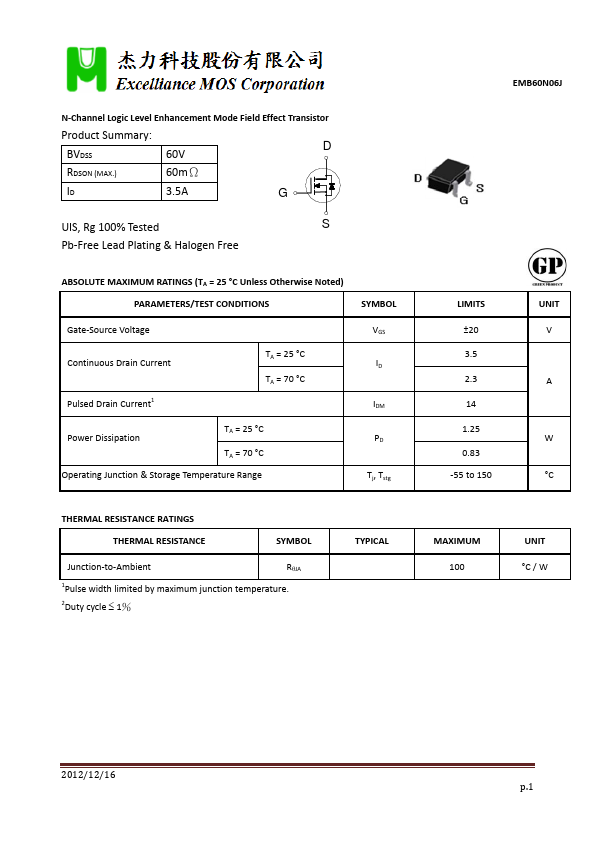
| Description | MOSFET |
| Category | MOSFET |
| Manufacturer | Excelliance MOS |
| Size | 167.47 KB |
| Seller | Inventory | Price Breaks | Buy |
|---|---|---|---|
| UnikeyIC | 30000 | 3000+ : 0.0154 USD 6000+ : 0.0151 USD 9000+ : 0.0148 USD |
View Offer |
| Unikeyic (ICkey) | 30000 | 3000+ : 0.0154 USD 6000+ : 0.0151 USD 9000+ : 0.0148 USD |
View Offer |
| Part Number | Manufacturer | Description |
|---|---|---|
| EMB60N06A | VBsemi | N-Channel 60V MOSFET |