EMB70A08G
EMB70A08G is MOSFET manufactured by Excelliance MOS.
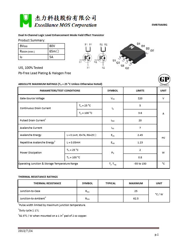
Dual N‐Channel Logic Level Enhancement Mode Field Effect Transistor
Product Summary:
BVDSS
80V
RDSON (MAX.)
65mΩ
5A
UIS, 100% Tested Pb‐Free Lead Plating & Halogen Free
ABSOLUTE MAXIMUM RATINGS (TA = 25 °C Unless Otherwise Noted) PARAMETERS/TEST CONDITIONS
SYMBOL
Gate‐Source Voltage
Continuous Drain Current Pulsed Drain Current1
TA = 25 °C TA = 100 °C
Avalanche Current
Avalanche Energy Repetitive Avalanche Energy2
L = 0.1m H, ID=7A, RG=25Ω
L = 0.05m H
Power Dissipation
TA = 25 °C TA = 100 °C
Operating Junction & Storage Temperature Range
VGS ID
IDM IAS EAS EAR PD
Tj, Tstg
THERMAL RESISTANCE RATINGS THERMAL RESISTANCE
SYMBOL
Junction‐to‐Case
RJC
Junction‐to‐Ambient3
RJA
1Pulse width limited by maximum junction temperature. 2Duty cycle 1% 362.5°C / W when mounted on a 1 in2 pad of 2 oz copper.
TYPICAL
LIMITS ±20 5 3.6 20 7 2.45 1.23 2 0.8
‐55 to 150
UNIT V A m J W °C
MAXIMUM 25 62.5
UNIT °C / W
2013/7/24 p.1
ELECTRICAL CHARACTERISTICS (TC = 25 °C, Unless Otherwise Noted)
PARAMETER...