EMD10N06A Overview
| Part | EMD10N06A |
|---|---|
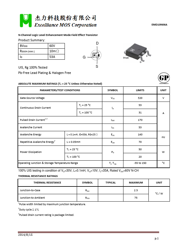
| Description | N-Channel Logic Level Enhancement Mode Field Effect Transistor |
| Category | Transistor |
| Manufacturer | Excelliance MOS |
| Size | 218.68 KB |
| Seller | Inventory | Price Breaks | Buy |
|---|---|---|---|
| UnikeyIC | 30000 | 2500+ : 0.0823 USD 5000+ : 0.0809 USD 7500+ : 0.0788 USD |
View Offer |
| Unikeyic (ICkey) | 30000 | 2500+ : 0.0823 USD 5000+ : 0.0809 USD 7500+ : 0.0788 USD |
View Offer |
| Part Number | Manufacturer | Description |
|---|---|---|
| BDT88 | Inchange Semiconductor | Silicon PNP Power Transistor |
| KD333 | Tesla Elektronicke | Transistor |
| C828 | SEMTECH | NPN Silicon Transistor |