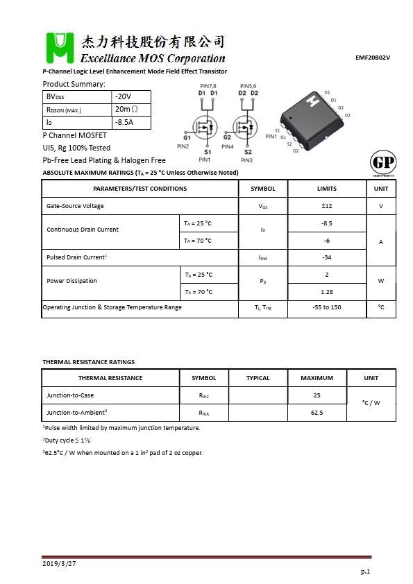
EMF20B02V Overview
Key Features
- 0.4 -0.75 -1.2
| Part | EMF20B02V |
|---|---|
| Description | P-Channel Logic Level Enhancement Mode Field Effect Transistor |
| Category | Transistor |
| Manufacturer | Excelliance MOS |
| Size | 852.57 KB |
| Seller | Inventory | Price Breaks | Buy |
|---|---|---|---|
| No distributor offers were returned for this part. | |||
| Part Number | Manufacturer | Description |
|---|---|---|
| BDT88 | Inchange Semiconductor | Silicon PNP Power Transistor |
| KD333 | Tesla Elektronicke | Transistor |
| C828 | SEMTECH | NPN Silicon Transistor |