FKCD3113
Description
The FKCD3113 bines advanced trench MOSFET technology with a low resistance package to provide extremely low RDSON. This device is ideal for load switch and battery protection applications. The FKCD3113 meet the Ro HS and Green Product requirement with full function reliability approved.
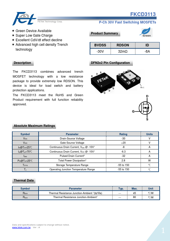
DFN2x2 Pin Configuration
Absolute Maximum Ratings
Symbol VDS VGS
ID@TA=25℃ ID@TA=70℃
IDM PD@TA=25℃
TSTG TJ
Parameter Drain-Source Voltage Gate-Source Voltage Continuous Drain Current, VGS @ -10V1 Continuous Drain Current, VGS @ -10V1 Pulsed Drain Current2 Total Power Dissipation3 Storage Temperature Range Operating Junction Temperature Range
Thermal Data
Symbol RθJA RθJA
Parameter Thermal Resistance Junction-Ambient 1(t≤10s)
Thermal Resistance Junction-Ambient1
Rating -30 ±20 -8 -6.3 -32 2.8
-55 to 150 -55 to 150
Units V V A A A W ℃ ℃
Typ. -----
Max. 45 80
Unit ℃/W ℃/W
Data and specifications subject to change without notice.
.fetek..tw Ver : A
FETek Technology...