FKD3018
FKD3018 is N-Channel MOSFET manufactured by FETek.
Description
The FKD3018 is the high cell density trenched N-ch MOSFETs, which provide excellent RDSON and gate charge for most applications. The FKD3018 meet the Ro HS and Green Product requirement, 100% EAS guaranteed with full function reliability approved.
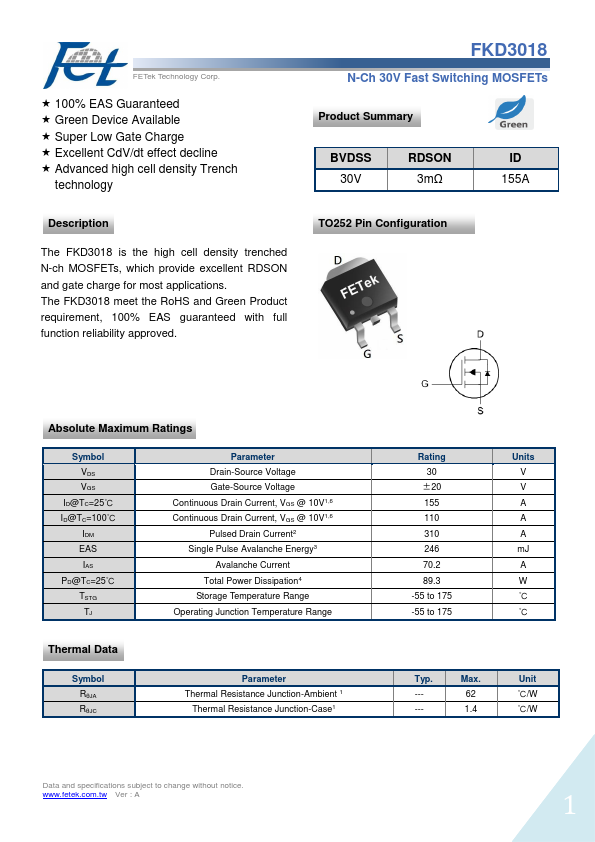
TO252 Pin Configuration
Absolute Maximum Ratings
Symbol VDS VGS
ID@TC=25℃ ID@TC=100℃
IDM EAS IAS PD@TC=25℃ TSTG
Parameter Drain-Source Voltage Gate-Source Voltage Continuous Drain Current, VGS @ 10V1,6 Continuous Drain Current, VGS @ 10V1,6 Pulsed Drain Current2 Single Pulse Avalanche Energy3
Avalanche Current Total Power Dissipation4 Storage Temperature Range Operating Junction Temperature Range
Thermal Data
Symbol RθJA RθJC
Parameter Thermal Resistance Junction-Ambient 1
Thermal Resistance Junction-Case1
Rating 30
±20 155 110 310 246 70.2 89.3 -55 to 175 -55 to 175
Units V V A A A m J A W ℃ ℃
Typ. -----
Max. 62 1.4
Unit ℃/W ℃/W
Data and specifications subject to change without notice.
.fetek..tw Ver : A
FETek Technology Corp.
N-Ch 30V Fast Switching MOSFETs
Electrical Characteristics (TJ=25 ℃, unless otherwise noted)
Symbol
Parameter
BVDSS Drain-Source Breakdown Voltage △BVDSS/△TJ BVDSS Temperature Coefficient
RDS(ON) Static Drain-Source On-Resistance2
VGS(th) △VGS(th)
Gate Threshold Voltage VGS(th) Temperature Coefficient
IDSS
Drain-Source Leakage Current
IGSS gfs Rg Qg Qgs Qgd Td(on) Tr Td(off) Tf Ciss Coss Crss
Gate-Source Leakage Current Forward Transconductance Gate Resistance Total Gate Charge (4.5V) Gate-Source Charge Gate-Drain Charge Turn-On Delay Time Rise Time Turn-Off Delay Time Fall Time Input Capacitance Output Capacitance Reverse Transfer Capacitance
Conditions VGS=0V , ID=250u A Reference to 25℃ , ID=1m A VGS=10V , ID=30A VGS=4.5V , ID=15A VGS=VDS , ID =250u A VDS=24V , VGS=0V , TJ=25℃ VDS=24V , VGS=0V , TJ=55℃ VGS=±20V , VDS=0V VDS=5V , ID=30A VDS=0V , VGS=0V , f=1MHz
VDS=15V , VGS=10V , ID=15A
VDD=15V , VGS=10V , RG=3.3, ID=1A
VDS=15V , VGS=0V ,...