FKK4008
FKK4008 is N-Channel MOSFET manufactured by FETek.
Description
The FKK4008 is the high cell density trenched N-ch MOSFETs, which provides excellent RDSON and efficiency for most of the small power switching and load switch applications. The FKK4008 meet the Ro HS and Green Product requirement with full function reliability approved.
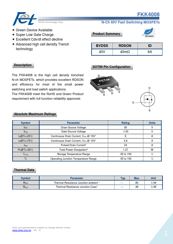
SOT89 Pin Configuration
Absolute Maximum Ratings
Symbol VDS VGS
ID@TA=25℃ ID@TA=70℃
IDM PD@TA=25℃
TSTG TJ
Parameter Drain-Source Voltage Gate-Source Voltage Continuous Drain Current, VGS @ 10V1 Continuous Drain Current, VGS @ 10V1 Pulsed Drain Current2 Total Power Dissipation3 Storage Temperature Range Operating Junction Temperature Range
Thermal Data
Symbol RθJA RθJC
Parameter Thermal Resistance Junction-ambient 1
Thermal Resistance Junction-Case1
Rating 40
±20 6 4.8 24
1.47 -55 to 150 -55 to 150
Units V V A A A W ℃ ℃
Typ. -----
Max. 85 48
Unit ℃/W ℃/W
Data and specifications subject to change without notice.
.fetek..tw Ver : A
FETek Technology Corp.
N-Ch 40V Fast Switching MOSFETs
Electrical Characteristics (TJ=25 ℃, unless otherwise noted)
Symbol
Parameter
BVDSS Drain-Source Breakdown Voltage △BVDSS/△TJ BVDSS Temperature Coefficient
RDS(ON) Static Drain-Source On-Resistance2
VGS(th) △VGS(th)
Gate Threshold Voltage VGS(th) Temperature Coefficient
IDSS
Drain-Source Leakage Current
IGSS gfs Rg Qg Qgs Qgd Td(on) Tr Td(off) Tf Ciss Coss Crss
Gate-Source Leakage Current Forward Transconductance Gate Resistance Total Gate Charge (4.5V) Gate-Source Charge Gate-Drain Charge Turn-On Delay Time Rise Time Turn-Off Delay Time Fall Time Input Capacitance Output Capacitance Reverse Transfer Capacitance
Conditions VGS=0V , ID=250u A Reference to 25℃ , ID=1m A VGS=10V , ID=4A VGS=4.5V , ID=3A VGS=VDS , ID =250u A VDS=32V , VGS=0V , TJ=25℃ VDS=32V , VGS=0V , TJ=55℃ VGS=±20V , VDS=0V VDS=5V , ID=4A VDS=0V , VGS=0V , f=1MHz
VDS=15V , VGS=4.5V , ID=3A
VDD=15V , VGS=10V , RG=3.3 ID=1A
VDS=15V , VGS=0V , f=1MHz
Min. 40 ------1.0 ---------------------------------...