4050B
Description
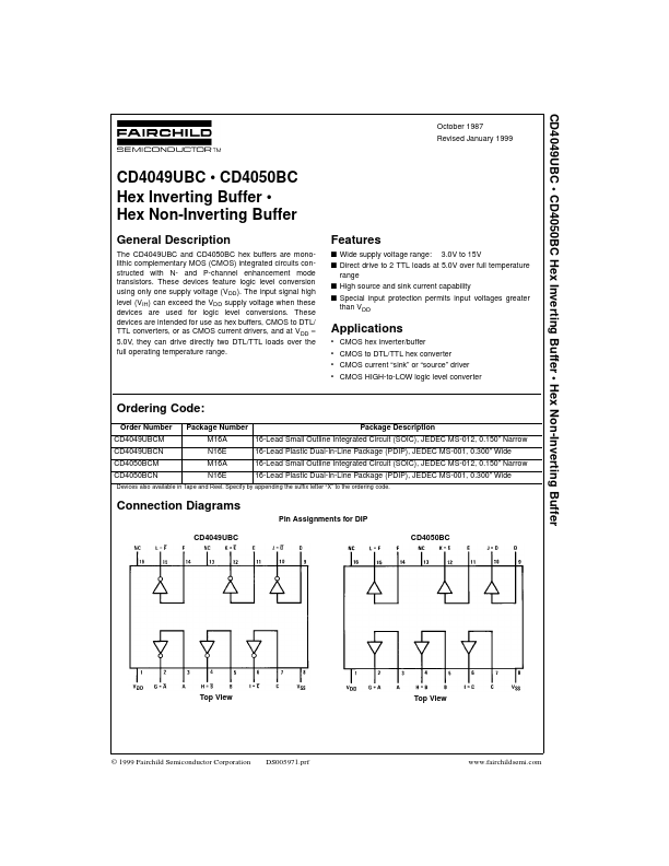
The CD4049UBC and CD4050BC hex buffers are monolithic plementary MOS (CMOS) integrated circuits constructed with N- and P-channel enhancement mode transistors. These devices feature logic level conversion using only one supply voltage (VDD ). The input signal high level (VIH) can exceed the VDD supply voltage when these devices are used for logic level conversions. These devices are intended for use as hex buffers, CMOS to DTL/ TTL converters, or as CMOS current drivers, and at VDD = 5.0V, they can drive directly two DTL/TTL loads over the full operating temperature range.
Features s Wide supply voltage range: 3.0V to 15V s Direct drive to 2 TTL loads at 5.0V over full temperature range s High source and sink current capability s Special input protection permits input voltages greater than VDD
Applications
- CMOS hex inverter/buffer
- CMOS to DTL/TTL hex converter
- CMOS current “sink” or “source” driver
- CMOS HIGH-to-LOW logic level converter
Ordering Code:
Order...