GENERAL DESCRIPTION
Address inputs are buffered to minimize loading and are fully decoded on-chip. The outputs are active only in the Read mode and the output data is the complement of the stored data. FEATURES
s 3-STATE outputs for data bus applications s Buffered inputs minimize loading s Address decoding on-chip s Diode clamped inputs minimize ringing Ordering Code: Order Number 74F189SC 74F189SJ 74F189PC (Note 1) Package Number M16B M16D N16E Package DESCRIPTION
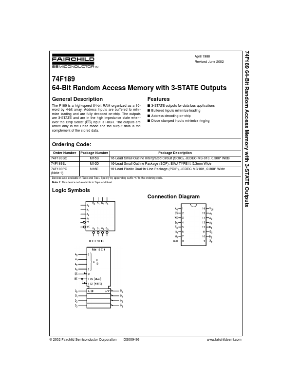
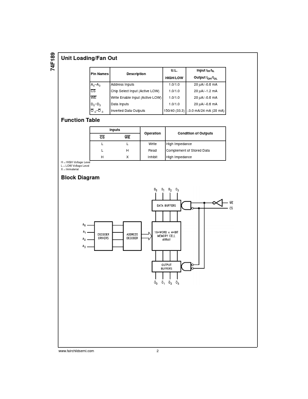
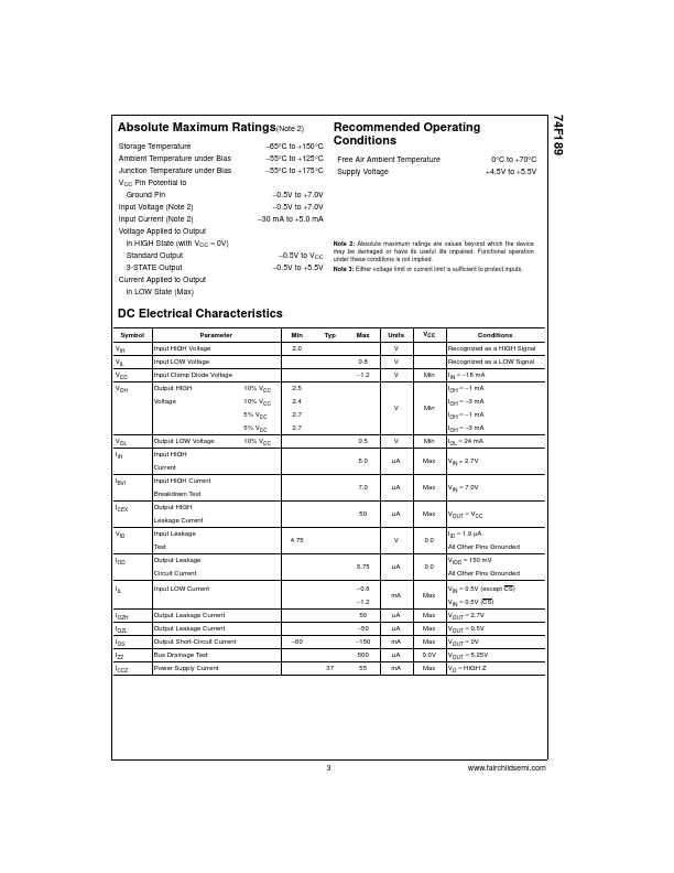
16-Lead Small Outline Intergrated Circuit (SOIC), JEDEC MS-013, 0.300" Wide 16-Lead Small Outline Package (SOP), EIAJ TYPE II, 5.3mm Wide 16-Lead Plastic Dual-In-Line Package (PDIP), JEDEC MS-001, 0.300" Wide Devices also available in Tape and Reel. Specify by appending suffix “X” to the ordering code. Note 1: This device not available in Tape and Reel. Logic Symbols Connection Diagram IEEE/IEC © 2002 Fairchild Semiconductor Corporation DS009493 74F189 Unit Loading/Fan Out U.L. Pin Names A0–A3 CS WE D0–D3 O 0–O 3 Descriptio... Fairchild Semiconductor