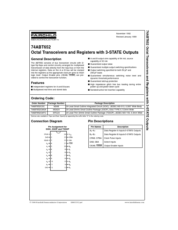
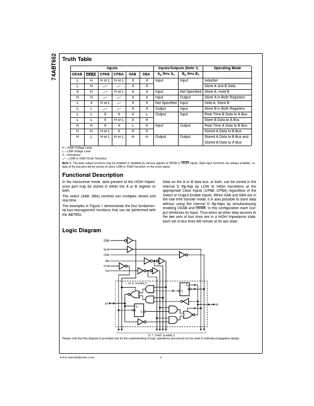
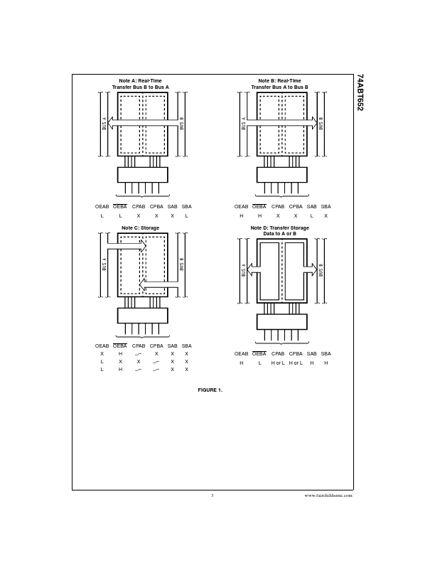
GENERAL DESCRIPTION
Data on the A or B bus will be clocked into the registers as the appropriate clock pin goes to HIGH logic level. Output Enable pins (OEAB, OEBA) are provided to control the transceiver function. FEATURES
s Independent registers for A and B buses s Multiplexed real-time and stored data s A and B output sink capability of 64 mA, source capability of 32 mA s Guaranteed output skew s Guaranteed multiple output switching specifications s Output switching specified for both 50 pF and 250 pF loads s Guaranteed simultaneous switching noise level and dynamic threshold performance s Guaranteed latchup protection s High Fairchild Semiconductor