74ALVC16240 Overview
Key Specifications
Package: TSSOP
Mount Type: Surface Mount
Pins: 48
Operating Voltage: 1.8 V
Description
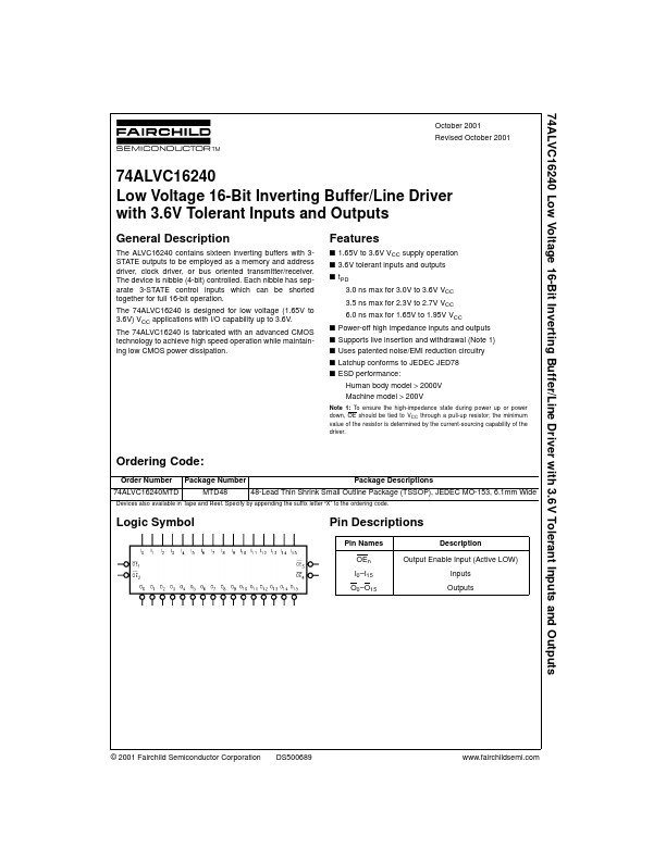
The ALVC16240 contains sixteen inverting buffers with 3STATE outputs to be employed as a memory and address driver, clock driver, or bus oriented transmitter/receiver. The device is nibble (4-bit) controlled.
Key Features
- Specify by appending the suffix letter “X” to the ordering code