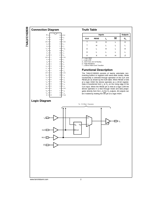
Datasheet4U Logo Datasheet4U.com

74ALVC162839 - Low Voltage 20-Bit Selectable Register/Buffer

General Description

The ALVC162839 contains twenty non-inverting selectable buffered or registered paths.

The device can be configured to operate in a registered, or flow through buffer mode by utilizing the register enable (REGE) and Clock (CLK) signals.

The device operates in a 20-bit word wide mode.

Key Features

  • s Compatible with PC100 and PC133 DIMM module specifications s 1.65V.
  • 3.6V VCC supply operation s 3.6V tolerant inputs and outputs s 26Ω series resistors in the outputs s tPD (CLK to O n) 4.6 ns max for 3.0V to 3.6V VCC 6.3 ns max for 2.3V to 2.7V VCC 9.8 ns max for 1.65V to 1.95V VCC s Power-off high impedance inputs and outputs s Supports live insertion and withdrawal (Note 1) s Uses patented noise/EMI reduction circuitry s Latchup conforms to JEDEC JED78 s ESD performance: Human body m.

📥 Download Datasheet

Full PDF Text Transcription (Reference)

The following content is an automatically extracted verbatim text from the original manufacturer datasheet and is provided for reference purposes only.

View original datasheet text
74ALVC162839 Low Voltage 20-Bit Selectable Register/Buffer with 3.6V Tolerant Inputs/Outputs and 26Ω Series Resistors in the Outputs November 2001 Revised November 2001 74ALVC162839 Low Voltage 20-Bit Selectable Register/Buffer with 3.6V Tolerant Inputs/Outputs and 26Ω Series Resistors in the Outputs General Description The ALVC162839 contains twenty non-inverting selectable buffered or registered paths. The device can be configured to operate in a registered, or flow through buffer mode by utilizing the register enable (REGE) and Clock (CLK) signals. The device operates in a 20-bit word wide mode. All outputs can be placed into 3-STATE through use of the OE pin. These devices are ideally suited for buffered or registered 168 pin and 200 pin SDRAM DIMM memory modules.