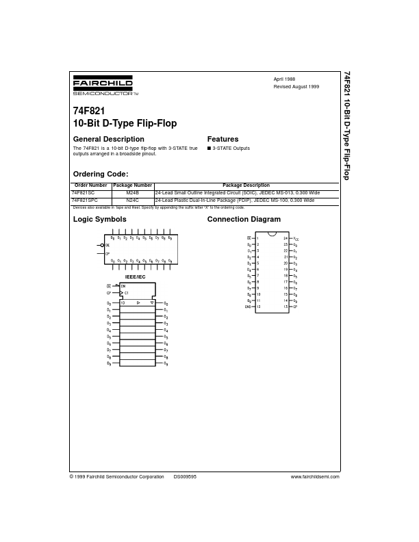
GENERAL DESCRIPTION
FEATURES
s 3-STATE Outputs Ordering Code: Order Number 74F821SC 74F821SPC Package Number M24B N24C Package DESCRIPTION
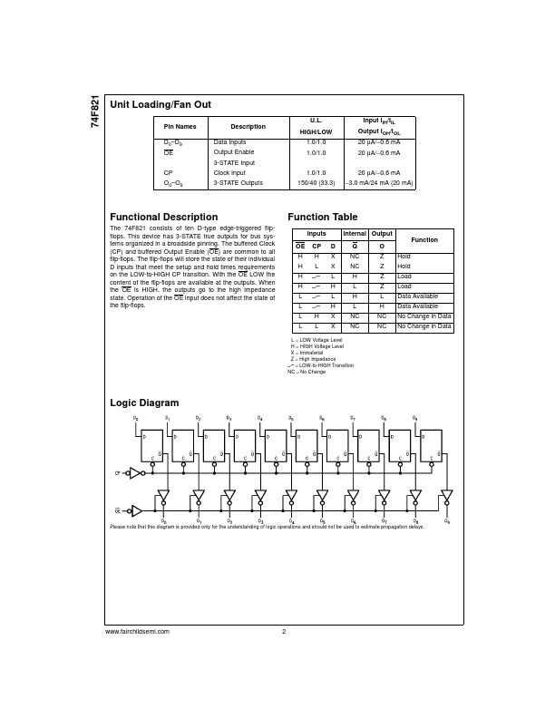
24-Lead Small Outline Integrated Circuit (SOIC), JEDEC MS-013, 0.300 Wide 24-Lead Plastic Dual-In-Line Package (PDIP), JEDEC MS-100, 0.300 Wide Devices also available in Tape and Reel. Specify by appending the suffix letter “X” to the ordering code. Logic Symbols Connection Diagram IEEE/IEC © 1999 Fairchild Semiconductor Corporation DS009595 74F821 Unit Loading/Fan Out Pin Names D0–D9 OE CP O0–O9 DESCRIPTION
Data Inputs Output Enable 3-STATE Input Clock Input 3-STATE Outputs 1.0/1.0 150/40 (33.3) 20 µA/−0.6 mA −3.0 mA/24 mA (20 mA) U.L. This device has 3-STATE true outputs for bus systems organized in a broadside pinning. The buffered Clock (CP) and buffered Output Enable (OE) are common to all flip-flops. The flip-flops will store the state of their individual D inputs that meet the setup and hold times requirements on the LOW-to-HIGH CP transition. Fairchild Semiconductor