74LCX240 Overview
Key Specifications
Package: TSSOP
Mount Type: Surface Mount
Pins: 20
Operating Voltage: 2.5 V
Description
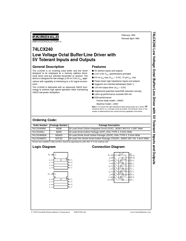
The LCX240 is an inverting octal buffer and line driver designed to be employed as a memory address driver, clock driver and bus oriented transmitter or receiver. The device is designed for low voltage (2.5V or 3.3V) VCC applications with capability of interfacing to a 5V signal environment.
Key Features
- Specify by appending the suffix letter “X” to the ordering code