74LCX652
Description
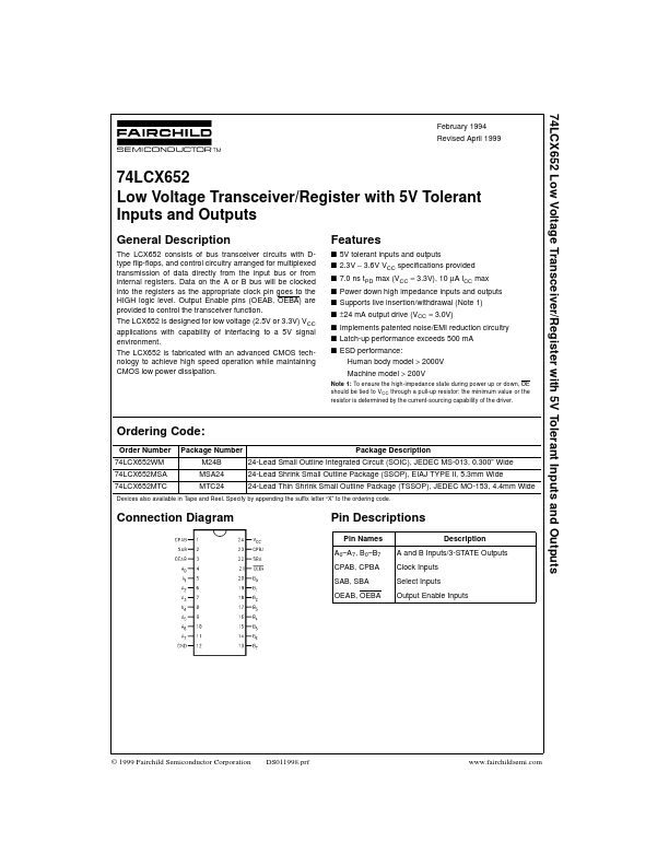
The LCX652 consists of bus transceiver circuits with Dtype flip-flops, and control circuitry arranged for multiplexed transmission of data directly from the input bus or from internal registers. Data on the A or B bus will be clocked into the registers as the appropriate clock pin goes to the HIGH logic level.
Key Features
- Specify by appending the suffix letter “X” to the ordering code
- Data input functions are always enabled, i.e., data at the bus pins will be stored on every LOW-to-HIGH transition on the clock inputs