GENERAL DESCRIPTION
Auxiliary inputs provided blanking, lamp test and cascadable zero-suppression functions. FEATURES
s Open-collector outputs s Drive indicator segments directly s Cascadable zero-suppression capability s Lamp test input Ordering Code: Order Number DM74LS47M DM74LS47N Package Number M16A N16E Package DESCRIPTION
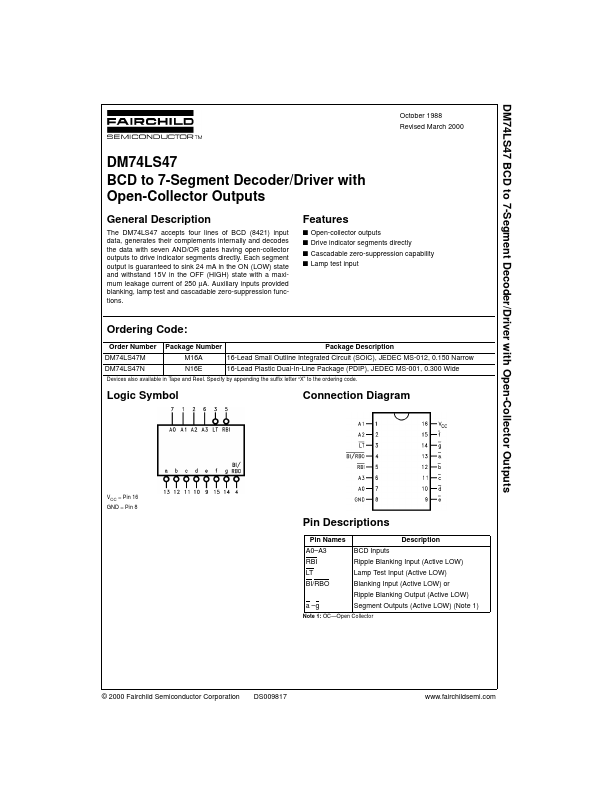
16-Lead Small Outline Integrated Circuit (SOIC), JEDEC MS-012, 0.150 Narrow 16-Lead Plastic Dual-In-Line Package (PDIP), JEDEC MS-001, 0.300 Wide Devices also available in Tape and Reel. Specify by appending the suffix letter “X” to the ordering code. Logic Symbol Connection Diagram VCC = Pin 16 GND = Pin 8 Pin Descriptions Pin Names A0–A3 RBI LT BI/RBO a –g BCD Inputs Ripple Blanking Input (Active LOW) Lamp Test Input (Active LOW) Blanking Input (Active LOW) or Ripple Blanking Output (Active LOW) Segment Outputs (Active LOW) (Note 1) Note 1: OC—Open Collector DESCRIPTION
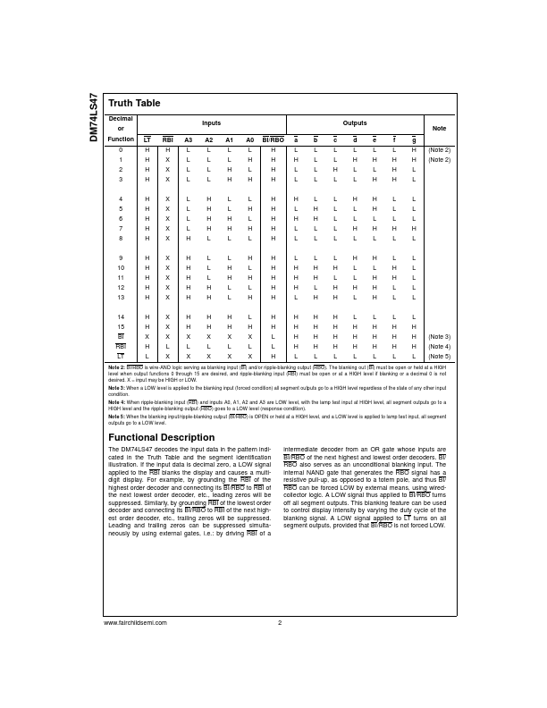
© 2000 Fairchild Semiconductor Corporation DS009817 DM74LS47 Truth Table Decimal or Functi... Fairchild Semiconductor