GENERAL DESCRIPTION
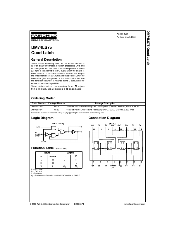
These latches are ideally suited for use as temporary storage for binary information between processing units and input/output or indicator units. Information present at a data (D) input is transferred to the Q output when the enable is HIGH, and the Q output will follow the data input as long as the enable remains HIGH. When the enable goes LOW, the information (that was present at the data input at the time the transition occurred) is retained at the Q output until the enable is permitted to go HIGH. These latches feature complementary Q and Q outputs from a 4-bit latch, and are available in 16-pin packages. Ordering Code: Order Number DM74LS75M DM74LS75N Package Number M16A N16E Package DESCRIPTION
16-Lead Small Outline Integrated Circuit (SOIC), JEDEC MS-012, 0.150 Narrow 16-Lead Plastic Dual-In-Line Package (PDIP), JEDEC MS-001, 0.300 Wide Devices also available in Tape and Reel. Specify by appending the suffix letter “X” to the ordering code. Logic Diagram (Ea... Fairchild Semiconductor